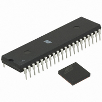
ATMEGA64RZAV-10PU Atmel, ATMEGA64RZAV-10PU Datasheet - Page 300

ATMEGA64RZAV-10PU
Manufacturer Part Number
ATMEGA64RZAV-10PU
Description
MCU ATMEGA644/AT86RF230 40-DIP
Manufacturer
Atmel
Series
ATMEGAr
Datasheets
1.ATMEGA644-20MU.pdf
(23 pages)
2.ATMEGA644-20MU.pdf
(376 pages)
3.AT86RF230-ZU.pdf
(98 pages)
Specifications of ATMEGA64RZAV-10PU
Frequency
2.4GHz
Modulation Or Protocol
802.15.4 Zigbee
Power - Output
3dBm
Sensitivity
-101dBm
Voltage - Supply
1.8 V ~ 3.6 V
Data Interface
PCB, Surface Mount
Memory Size
64kB Flash, 2kB EEPROM, 4kB RAM
Antenna Connector
PCB, Surface Mount
Package / Case
40-DIP (0.600", 15.24mm)
Wireless Frequency
2.4 GHz
Interface Type
JTAG, SPI
Output Power
3 dBm
For Use With
ATSTK600-TQFP32 - STK600 SOCKET/ADAPTER 32-TQFPATAVRISP2 - PROGRAMMER AVR IN SYSTEMATSTK500 - PROGRAMMER AVR STARTER KIT
Lead Free Status / RoHS Status
Lead free / RoHS Compliant
Operating Temperature
-
Applications
-
Data Rate - Maximum
-
Current - Transmitting
-
Current - Receiving
-
Lead Free Status / Rohs Status
Lead free / RoHS Compliant
For Use With/related Products
ATmega64
- Current page: 300 of 376
- Download datasheet (8Mb)
25.8.2
300
ATmega644
Serial Programming Algorithm
When programming the EEPROM, an auto-erase cycle is built into the self-timed programming
operation (in the Serial mode ONLY) and there is no need to first execute the Chip Erase
instruction. The Chip Erase operation turns the content of every memory location in both the
Program and EEPROM arrays into 0xFF.
Depending on CKSEL Fuses, a valid clock must be present. The minimum low and high periods
for the serial clock (SCK) input are defined as follows:
Low: > 2 CPU clock cycles for f
High: > 2 CPU clock cycles for f
When writing serial data to the ATmega644, data is clocked on the rising edge of SCK.
When reading data from the ATmega644, data is clocked on the falling edge of SCK. See
25-12
To program and verify the ATmega644 in the serial programming mode, the following sequence
is recommended (See four byte instruction formats in
1. Power-up sequence:
2. Wait for at least 20 ms and enable serial programming by sending the Programming
3. The serial programming instructions will not work if the communication is out of synchro-
4. The Flash is programmed one page at a time. The memory page is loaded one byte at a
5. The EEPROM array is programmed one byte at a time by supplying the address and data
6. Any memory location can be verified by using the Read instruction which returns the con-
Apply power between V
tems, the programmer can not guarantee that SCK is held low during power-up. In this
case, RESET must be given a positive pulse of at least two CPU clock cycles duration
after SCK has been set to “0”.
Enable serial instruction to pin MOSI.
nization. When in sync. the second byte (0x53), will echo back when issuing the third
byte of the Programming Enable instruction. Whether the echo is correct or not, all four
bytes of the instruction must be transmitted. If the 0x53 did not echo back, give RESET a
positive pulse and issue a new Programming Enable command.
time by supplying the 7 LSB of the address and data together with the Load Program
Memory Page instruction. To ensure correct loading of the page, the data low byte must
be loaded before data high byte is applied for a given address. The Program Memory
Page is stored by loading the Write Program Memory Page instruction with the address
lines 15..8. Before issuing this command, make sure the instruction Load Extended
Address Byte has been used to define the MSB of the address. The extended address
byte is stored until the command is re-issued, that is, the command needs only be issued
for the first page, and when crossing the 64KWord boundary. If polling (
used, the user must wait at least t
16.) Accessing the serial programming interface before the Flash write operation com-
pletes can result in incorrect programming.
together with the appropriate Write instruction. An EEPROM memory location is first
automatically erased before new data is written. If polling is not used, the user must wait
at least t
device, no 0xFFs in the data file(s) need to be programmed.
tent at the selected address at serial output MISO. When reading the Flash memory, use
the instruction Load Extended Address Byte to define the upper address byte, which is
not included in the Read Program Memory instruction. The extended address byte is
for timing details.
WD_EEPROM
before issuing the next byte. (See
CC
and GND while RESET and SCK are set to “0”. In some sys-
ck
ck
< 12 MHz, 3 CPU clock cycles for f
< 12 MHz, 3 CPU clock cycles for f
WD_FLASH
before issuing the next page. (See
Table
Table
25-17):
25-16.) In a chip erased
ck
ck
>= 12 MHz
>= 12 MHz
RDY/BSY
Table 25-
2593N–AVR–07/10
) is not
Figure
Related parts for ATMEGA64RZAV-10PU
Image
Part Number
Description
Manufacturer
Datasheet
Request
R

Part Number:
Description:
DEV KIT FOR AVR/AVR32
Manufacturer:
Atmel
Datasheet:

Part Number:
Description:
INTERVAL AND WIPE/WASH WIPER CONTROL IC WITH DELAY
Manufacturer:
ATMEL Corporation
Datasheet:

Part Number:
Description:
Low-Voltage Voice-Switched IC for Hands-Free Operation
Manufacturer:
ATMEL Corporation
Datasheet:

Part Number:
Description:
MONOLITHIC INTEGRATED FEATUREPHONE CIRCUIT
Manufacturer:
ATMEL Corporation
Datasheet:

Part Number:
Description:
AM-FM Receiver IC U4255BM-M
Manufacturer:
ATMEL Corporation
Datasheet:

Part Number:
Description:
Monolithic Integrated Feature Phone Circuit
Manufacturer:
ATMEL Corporation
Datasheet:

Part Number:
Description:
Multistandard Video-IF and Quasi Parallel Sound Processing
Manufacturer:
ATMEL Corporation
Datasheet:

Part Number:
Description:
High-performance EE PLD
Manufacturer:
ATMEL Corporation
Datasheet:

Part Number:
Description:
8-bit Flash Microcontroller
Manufacturer:
ATMEL Corporation
Datasheet:

Part Number:
Description:
2-Wire Serial EEPROM
Manufacturer:
ATMEL Corporation
Datasheet:


