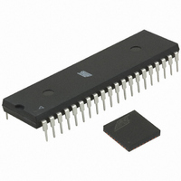
ATMEGA64RZAV-10PU Atmel, ATMEGA64RZAV-10PU Datasheet - Page 258

ATMEGA64RZAV-10PU
Manufacturer Part Number
ATMEGA64RZAV-10PU
Description
MCU ATMEGA644/AT86RF230 40-DIP
Manufacturer
Atmel
Series
ATMEGAr
Datasheets
1.ATMEGA644-20MU.pdf
(23 pages)
2.ATMEGA644-20MU.pdf
(376 pages)
3.AT86RF230-ZU.pdf
(98 pages)
Specifications of ATMEGA64RZAV-10PU
Frequency
2.4GHz
Modulation Or Protocol
802.15.4 Zigbee
Power - Output
3dBm
Sensitivity
-101dBm
Voltage - Supply
1.8 V ~ 3.6 V
Data Interface
PCB, Surface Mount
Memory Size
64kB Flash, 2kB EEPROM, 4kB RAM
Antenna Connector
PCB, Surface Mount
Package / Case
40-DIP (0.600", 15.24mm)
Wireless Frequency
2.4 GHz
Interface Type
JTAG, SPI
Output Power
3 dBm
For Use With
ATSTK600-TQFP32 - STK600 SOCKET/ADAPTER 32-TQFPATAVRISP2 - PROGRAMMER AVR IN SYSTEMATSTK500 - PROGRAMMER AVR STARTER KIT
Lead Free Status / RoHS Status
Lead free / RoHS Compliant
Operating Temperature
-
Applications
-
Data Rate - Maximum
-
Current - Transmitting
-
Current - Receiving
-
Lead Free Status / Rohs Status
Lead free / RoHS Compliant
For Use With/related Products
ATmega64
- Current page: 258 of 376
- Download datasheet (8Mb)
22.8
22.9
22.9.1
258
Bibliography
Register Description
ATmega644
OCDR – On-chip Debug Register
The JTAG programming capability supports:
• Flash programming and verifying.
• EEPROM programming and verifying.
• Fuse programming and verifying.
• Lock bit programming and verifying.
The Lock bit security is exactly as in parallel programming mode. If the Lock bits LB1 or LB2 are
programmed, the OCDEN Fuse cannot be programmed unless first doing a chip erase. This is a
security feature that ensures no back-door exists for reading out the content of a secured
device.
The details on programming through the JTAG interface and programming specific JTAG
instructions are given in the section
For more information about general Boundary-scan, the following literature can be consulted:
• IEEE: IEEE Std. 1149.1-1990. IEEE Standard Test Access Port and Boundary-scan
• Colin Maunder: The Board Designers Guide to Testable Logic Circuits, Addison-Wesley, 1992.
The OCDR Register provides a communication channel from the running program in the micro-
controller to the debugger. The CPU can transfer a byte to the debugger by writing to this
location. At the same time, an internal flag; I/O Debug Register Dirty – IDRD – is set to indicate
to the debugger that the register has been written. When the CPU reads the OCDR Register the
7 LSB will be from the OCDR Register, while the MSB is the IDRD bit. The debugger clears the
IDRD bit when it has read the information.
In some AVR devices, this register is shared with a standard I/O location. In this case, the OCDR
Register can only be accessed if the OCDEN Fuse is programmed, and the debugger enables
access to the OCDR Register. In all other cases, the standard I/O location is accessed.
Refer to the debugger documentation for further information on how to use this register.
Bit
0x31 (0x51)
Read/Write
Initial Value
Architecture, IEEE, 1993.
MSB/IDRD
R/W
7
0
R/W
6
0
”Programming via the JTAG Interface” on page
R/W
5
0
R/W
4
0
R/W
3
0
R/W
2
0
R/W
1
0
LSB
R/W
0
0
2593N–AVR–07/10
303.
OCDR
Related parts for ATMEGA64RZAV-10PU
Image
Part Number
Description
Manufacturer
Datasheet
Request
R

Part Number:
Description:
DEV KIT FOR AVR/AVR32
Manufacturer:
Atmel
Datasheet:

Part Number:
Description:
INTERVAL AND WIPE/WASH WIPER CONTROL IC WITH DELAY
Manufacturer:
ATMEL Corporation
Datasheet:

Part Number:
Description:
Low-Voltage Voice-Switched IC for Hands-Free Operation
Manufacturer:
ATMEL Corporation
Datasheet:

Part Number:
Description:
MONOLITHIC INTEGRATED FEATUREPHONE CIRCUIT
Manufacturer:
ATMEL Corporation
Datasheet:

Part Number:
Description:
AM-FM Receiver IC U4255BM-M
Manufacturer:
ATMEL Corporation
Datasheet:

Part Number:
Description:
Monolithic Integrated Feature Phone Circuit
Manufacturer:
ATMEL Corporation
Datasheet:

Part Number:
Description:
Multistandard Video-IF and Quasi Parallel Sound Processing
Manufacturer:
ATMEL Corporation
Datasheet:

Part Number:
Description:
High-performance EE PLD
Manufacturer:
ATMEL Corporation
Datasheet:

Part Number:
Description:
8-bit Flash Microcontroller
Manufacturer:
ATMEL Corporation
Datasheet:

Part Number:
Description:
2-Wire Serial EEPROM
Manufacturer:
ATMEL Corporation
Datasheet:


