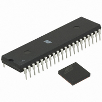
ATMEGA64RZAV-10PU Atmel, ATMEGA64RZAV-10PU Datasheet - Page 303

ATMEGA64RZAV-10PU
Manufacturer Part Number
ATMEGA64RZAV-10PU
Description
MCU ATMEGA644/AT86RF230 40-DIP
Manufacturer
Atmel
Series
ATMEGAr
Datasheets
1.ATMEGA644-20MU.pdf
(23 pages)
2.ATMEGA644-20MU.pdf
(376 pages)
3.AT86RF230-ZU.pdf
(98 pages)
Specifications of ATMEGA64RZAV-10PU
Frequency
2.4GHz
Modulation Or Protocol
802.15.4 Zigbee
Power - Output
3dBm
Sensitivity
-101dBm
Voltage - Supply
1.8 V ~ 3.6 V
Data Interface
PCB, Surface Mount
Memory Size
64kB Flash, 2kB EEPROM, 4kB RAM
Antenna Connector
PCB, Surface Mount
Package / Case
40-DIP (0.600", 15.24mm)
Wireless Frequency
2.4 GHz
Interface Type
JTAG, SPI
Output Power
3 dBm
For Use With
ATSTK600-TQFP32 - STK600 SOCKET/ADAPTER 32-TQFPATAVRISP2 - PROGRAMMER AVR IN SYSTEMATSTK500 - PROGRAMMER AVR STARTER KIT
Lead Free Status / RoHS Status
Lead free / RoHS Compliant
Operating Temperature
-
Applications
-
Data Rate - Maximum
-
Current - Transmitting
-
Current - Receiving
-
Lead Free Status / Rohs Status
Lead free / RoHS Compliant
For Use With/related Products
ATmega64
- Current page: 303 of 376
- Download datasheet (8Mb)
25.9.1
25.10 Programming via the JTAG Interface
25.10.1
2593N–AVR–07/10
Serial Programming Characteristics
Programming Specific JTAG Instructions
For characteristics of the Serial Programming module see “SPI Timing Characteristics” on page
322.
Figure 25-12. Serial Programming Waveforms
Programming through the JTAG interface requires control of the four JTAG specific pins: TCK,
TMS, TDI, and TDO. Control of the reset and clock pins is not required.
To be able to use the JTAG interface, the JTAGEN Fuse must be programmed. The device is
default shipped with the fuse programmed. In addition, the JTD bit in MCUCSR must be cleared.
Alternatively, if the JTD bit is set, the external reset can be forced low. Then, the JTD bit will be
cleared after two chip clocks, and the JTAG pins are available for programming. This provides a
means of using the JTAG pins as normal port pins in Running mode while still allowing In-Sys-
tem Programming via the JTAG interface. Note that this technique can not be used when using
the JTAG pins for Boundary-scan or On-chip Debug. In these cases the JTAG pins must be ded-
icated for this purpose.
During programming the clock frequency of the TCK Input must be less than the maximum fre-
quency of the chip. The System Clock Prescaler can not be used to divide the TCK Clock Input
into a sufficiently low frequency.
As a definition in this datasheet, the LSB is shifted in and out first of all Shift Registers.
The Instruction Register is 4-bit wide, supporting up to 16 instructions. The JTAG instructions
useful for programming are listed below.
The OPCODE for each instruction is shown behind the instruction name in hex format. The text
describes which Data Register is selected as path between TDI and TDO for each instruction.
The Run-Test/Idle state of the TAP controller is used to generate internal clocks. It can also be
used as an idle state between JTAG sequences. The state machine sequence for changing the
instruction word is shown in
SERIAL DATA OUTPUT
SERIAL CLOCK INPUT
SERIAL DATA INPUT
SAMPLE
(MOSI)
(MISO)
(SCK)
Figure
MSB
MSB
25-13.
ATmega644
LSB
LSB
303
Related parts for ATMEGA64RZAV-10PU
Image
Part Number
Description
Manufacturer
Datasheet
Request
R

Part Number:
Description:
DEV KIT FOR AVR/AVR32
Manufacturer:
Atmel
Datasheet:

Part Number:
Description:
INTERVAL AND WIPE/WASH WIPER CONTROL IC WITH DELAY
Manufacturer:
ATMEL Corporation
Datasheet:

Part Number:
Description:
Low-Voltage Voice-Switched IC for Hands-Free Operation
Manufacturer:
ATMEL Corporation
Datasheet:

Part Number:
Description:
MONOLITHIC INTEGRATED FEATUREPHONE CIRCUIT
Manufacturer:
ATMEL Corporation
Datasheet:

Part Number:
Description:
AM-FM Receiver IC U4255BM-M
Manufacturer:
ATMEL Corporation
Datasheet:

Part Number:
Description:
Monolithic Integrated Feature Phone Circuit
Manufacturer:
ATMEL Corporation
Datasheet:

Part Number:
Description:
Multistandard Video-IF and Quasi Parallel Sound Processing
Manufacturer:
ATMEL Corporation
Datasheet:

Part Number:
Description:
High-performance EE PLD
Manufacturer:
ATMEL Corporation
Datasheet:

Part Number:
Description:
8-bit Flash Microcontroller
Manufacturer:
ATMEL Corporation
Datasheet:

Part Number:
Description:
2-Wire Serial EEPROM
Manufacturer:
ATMEL Corporation
Datasheet:


