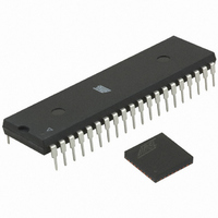
ATMEGA64RZAV-10PU Atmel, ATMEGA64RZAV-10PU Datasheet - Page 251

ATMEGA64RZAV-10PU
Manufacturer Part Number
ATMEGA64RZAV-10PU
Description
MCU ATMEGA644/AT86RF230 40-DIP
Manufacturer
Atmel
Series
ATMEGAr
Datasheets
1.ATMEGA644-20MU.pdf
(23 pages)
2.ATMEGA644-20MU.pdf
(376 pages)
3.AT86RF230-ZU.pdf
(98 pages)
Specifications of ATMEGA64RZAV-10PU
Frequency
2.4GHz
Modulation Or Protocol
802.15.4 Zigbee
Power - Output
3dBm
Sensitivity
-101dBm
Voltage - Supply
1.8 V ~ 3.6 V
Data Interface
PCB, Surface Mount
Memory Size
64kB Flash, 2kB EEPROM, 4kB RAM
Antenna Connector
PCB, Surface Mount
Package / Case
40-DIP (0.600", 15.24mm)
Wireless Frequency
2.4 GHz
Interface Type
JTAG, SPI
Output Power
3 dBm
For Use With
ATSTK600-TQFP32 - STK600 SOCKET/ADAPTER 32-TQFPATAVRISP2 - PROGRAMMER AVR IN SYSTEMATSTK500 - PROGRAMMER AVR STARTER KIT
Lead Free Status / RoHS Status
Lead free / RoHS Compliant
Operating Temperature
-
Applications
-
Data Rate - Maximum
-
Current - Transmitting
-
Current - Receiving
-
Lead Free Status / Rohs Status
Lead free / RoHS Compliant
For Use With/related Products
ATmega64
- Current page: 251 of 376
- Download datasheet (8Mb)
21.9.3
ADLAR = 0
ADLAR = 1
21.9.4
2593N–AVR–07/10
ADCL and ADCH – The ADC Data Register
ADCSRB – ADC Control and Status Register B
When an ADC conversion is complete, the result is found in these two registers. If differential
channels are used, the result is presented in two’s complement form.
When ADCL is read, the ADC Data Register is not updated until ADCH is read. Consequently, if
the result is left adjusted and no more than 8-bit precision is required, it is sufficient to read
ADCH. Otherwise, ADCL must be read first, then ADCH.
The ADLAR bit in ADMUX, and the MUXn bits in ADMUX affect the way the result is read from
the registers. If ADLAR is set, the result is left adjusted. If ADLAR is cleared (default), the result
is right adjusted.
• ADC9:0: ADC Conversion Result
These bits represent the result from the conversion, as detailed in
page
• Bit 7, 5:3 – Res: Reserved Bits
These bits are reserved for future use in the ATmega644. For ensuring compability with future
devices, these bits must be written zero when ADCSRB is written.
• Bit 2:0 – ADTS2:0: ADC Auto Trigger Source
If ADATE in ADCSRA is written to one, the value of these bits selects which source will trigger
an ADC conversion. If ADATE is cleared, the ADTS[2:0] settings will have no effect. A conver-
sion will be triggered by the rising edge of the selected Interrupt Flag. Note that switching from a
trigger source that is cleared to a trigger source that is set, will generate a positive edge on the
Bit
(0x79)
(0x78)
Read/Write
Initial Value
Bit
(0x79)
(0x78)
Read/Write
Initial Value
Bit
(0x7B)
Read/Write
Initial Value
246.
ADC7
ADC9
ADC1
15
15
R
R
R
R
–
7
0
0
7
0
0
R
7
–
0
ACME
ADC6
ADC8
ADC0
R/W
14
14
R
R
R
R
–
6
0
0
6
0
0
6
0
ADC5
ADC7
13
13
R
R
R
R
R
–
5
0
0
–
5
0
0
5
–
0
ADC4
ADC6
12
12
R
R
R
R
–
4
0
0
–
4
0
0
R
4
–
0
ADC3
ADC5
11
11
R
R
R
R
–
3
0
0
–
3
0
0
R
3
–
0
ADTS2
ADC2
ADC4
R/W
10
10
R
R
R
R
–
2
0
0
–
2
0
0
2
0
”ADC Conversion Result” on
ADTS1
ADC9
ADC1
ADC3
R/W
R
R
R
R
9
1
0
0
9
–
1
0
0
1
0
ATmega644
ADTS0
ADC8
ADC0
ADC2
R/W
R
R
R
R
8
0
0
0
8
–
0
0
0
0
0
ADCSRB
ADCH
ADCH
ADCL
ADCL
251
Related parts for ATMEGA64RZAV-10PU
Image
Part Number
Description
Manufacturer
Datasheet
Request
R

Part Number:
Description:
DEV KIT FOR AVR/AVR32
Manufacturer:
Atmel
Datasheet:

Part Number:
Description:
INTERVAL AND WIPE/WASH WIPER CONTROL IC WITH DELAY
Manufacturer:
ATMEL Corporation
Datasheet:

Part Number:
Description:
Low-Voltage Voice-Switched IC for Hands-Free Operation
Manufacturer:
ATMEL Corporation
Datasheet:

Part Number:
Description:
MONOLITHIC INTEGRATED FEATUREPHONE CIRCUIT
Manufacturer:
ATMEL Corporation
Datasheet:

Part Number:
Description:
AM-FM Receiver IC U4255BM-M
Manufacturer:
ATMEL Corporation
Datasheet:

Part Number:
Description:
Monolithic Integrated Feature Phone Circuit
Manufacturer:
ATMEL Corporation
Datasheet:

Part Number:
Description:
Multistandard Video-IF and Quasi Parallel Sound Processing
Manufacturer:
ATMEL Corporation
Datasheet:

Part Number:
Description:
High-performance EE PLD
Manufacturer:
ATMEL Corporation
Datasheet:

Part Number:
Description:
8-bit Flash Microcontroller
Manufacturer:
ATMEL Corporation
Datasheet:

Part Number:
Description:
2-Wire Serial EEPROM
Manufacturer:
ATMEL Corporation
Datasheet:


