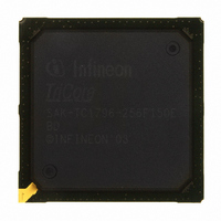
SAK-TC1796-256F150E BD Infineon Technologies, SAK-TC1796-256F150E BD Datasheet - Page 95

SAK-TC1796-256F150E BD
Manufacturer Part Number
SAK-TC1796-256F150E BD
Description
IC MCU 32BIT FLASH PG-BGA-416
Manufacturer
Infineon Technologies
Series
TC17xxr
Datasheet
1.SAK-TC1796-256F150E_BE.pdf
(134 pages)
Specifications of SAK-TC1796-256F150E BD
Core Processor
TriCore
Core Size
32-Bit
Speed
150MHz
Connectivity
ASC, CAN, EBI/EMI, MLI, MSC, SSC
Peripherals
DMA, POR, WDT
Number Of I /o
123
Program Memory Size
2MB (2M x 8)
Program Memory Type
FLASH
Ram Size
256K x 8
Voltage - Supply (vcc/vdd)
1.42 V ~ 1.58 V
Data Converters
A/D 44x12b
Oscillator Type
External
Operating Temperature
-40°C ~ 125°C
Package / Case
416-BGA
Packages
PG-BGA-416
Max Clock Frequency
150.0 MHz
Sram (incl. Cache)
256.0 KByte
Can Nodes
4
A / D Input Lines (incl. Fadc)
44
Program Memory
2.0 MB
For Use With
B158-H8537-G2-X-7600IN - KIT STARTER TC179X FAMILY
Lead Free Status / RoHS Status
Lead free / RoHS Compliant
Eeprom Size
-
Other names
KT1796256F150EBDXP
SAK-TC1796-256F150EBDIN
SP000228336
SAK-TC1796-256F150EBDIN
SP000228336
- Current page: 95 of 134
- Download datasheet (5Mb)
8) ADC module capability.
9) Not subject to production test, verified by design / characterization.
10) Value under typical application conditions due to integration (switching noise, etc.).
11) The sum of DNL/INL/Gain/Offset errors does not exceed the related TUE total unadjusted error.
12) For 10-bit conversions the DNL/INL/Gain/Offset error values must be multiplied with factor 0.25.
13) The leakage current definition is a continuous function, as shown in
14) Only one of these parameters is tested, the other is verified by design characterization.
15)
16) For the definition of the parameters see also
17) Applies to AIN0 and AIN1, when used as auxiliary reference inputs.
18) This represents an equivalent switched capacitance. This capacitance is not switched to the reference voltage
19) The sampling capacity of the conversion C-Network is pre-charged to
Data Sheet
For 8-bit conversions the DNL/INL/Gain/Offset error values must be multiplied with 0.0625.
determine the characteristic points of the given continuous linear approximation - they do not define step
function.
I
with a duration of up to
needs a total charge of
All ADC conversions with a duration longer than
at once. Instead of this smaller capacitances are successively switched to the reference voltage.
Because of the parasitic elements the voltage measured at AINx is lower then
AREF_MAX
is valid for the minimum specified conversion time. The current flowing during an ADC conversion
Q
t
C
CONV
= 25µs can be calculated with the formula
= 150pC from
V
Figure
AREF
t
C
.
95
= 25µs consume an
23.
Figure
I
AREF_MAX
V
I
AREF_MAX
AREF
24. The numerical values defined
/2 before the sampling moment.
V
Electrical Parameters
=
AREF
Q
= 6µA.
CONV
/2, typically 0.85V.
/
t
C
. Every conversion
V1.0, 2008-04
TC1796
Related parts for SAK-TC1796-256F150E BD
Image
Part Number
Description
Manufacturer
Datasheet
Request
R

Part Number:
Description:
IC MCU 32BIT FLASH 416-BGA
Manufacturer:
Infineon Technologies
Datasheet:

Part Number:
Description:
IC MCU 32BIT FLASH BGA-416
Manufacturer:
Infineon Technologies
Datasheet:

Part Number:
Description:
Manufacturer:
Infineon Technologies AG
Datasheet:

Part Number:
Description:
BGA 416/32 BIT FLASH
Manufacturer:
Infineon Technologies AG
Datasheet:

Part Number:
Description:
Manufacturer:
Infineon Technologies AG
Datasheet:

Part Number:
Description:
Manufacturer:
Infineon Technologies AG
Datasheet:

Part Number:
Description:
Manufacturer:
Infineon Technologies AG
Datasheet:

Part Number:
Description:
Manufacturer:
Infineon Technologies AG
Datasheet:

Part Number:
Description:
Manufacturer:
Infineon Technologies AG
Datasheet:

Part Number:
Description:
Manufacturer:
Infineon Technologies AG
Datasheet:

Part Number:
Description:
Manufacturer:
Infineon Technologies AG
Datasheet:

Part Number:
Description:
16-bit microcontroller with 2x2 KByte RAM
Manufacturer:
Infineon Technologies AG
Datasheet:

Part Number:
Description:
NPN silicon RF transistor
Manufacturer:
Infineon Technologies AG
Datasheet:

Part Number:
Description:
NPN silicon RF transistor
Manufacturer:
Infineon Technologies AG
Datasheet:

Part Number:
Description:
NPN silicon RF transistor
Manufacturer:
Infineon Technologies AG
Datasheet:


