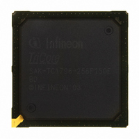
SAK-TC1796-256F150E BD Infineon Technologies, SAK-TC1796-256F150E BD Datasheet - Page 94

SAK-TC1796-256F150E BD
Manufacturer Part Number
SAK-TC1796-256F150E BD
Description
IC MCU 32BIT FLASH PG-BGA-416
Manufacturer
Infineon Technologies
Series
TC17xxr
Datasheet
1.SAK-TC1796-256F150E_BE.pdf
(134 pages)
Specifications of SAK-TC1796-256F150E BD
Core Processor
TriCore
Core Size
32-Bit
Speed
150MHz
Connectivity
ASC, CAN, EBI/EMI, MLI, MSC, SSC
Peripherals
DMA, POR, WDT
Number Of I /o
123
Program Memory Size
2MB (2M x 8)
Program Memory Type
FLASH
Ram Size
256K x 8
Voltage - Supply (vcc/vdd)
1.42 V ~ 1.58 V
Data Converters
A/D 44x12b
Oscillator Type
External
Operating Temperature
-40°C ~ 125°C
Package / Case
416-BGA
Packages
PG-BGA-416
Max Clock Frequency
150.0 MHz
Sram (incl. Cache)
256.0 KByte
Can Nodes
4
A / D Input Lines (incl. Fadc)
44
Program Memory
2.0 MB
For Use With
B158-H8537-G2-X-7600IN - KIT STARTER TC179X FAMILY
Lead Free Status / RoHS Status
Lead free / RoHS Compliant
Eeprom Size
-
Other names
KT1796256F150EBDXP
SAK-TC1796-256F150EBDIN
SP000228336
SAK-TC1796-256F150EBDIN
SP000228336
- Current page: 94 of 134
- Download datasheet (5Mb)
Table 15
Parameter
Resistance of the
reference voltage
input path
Total capacitance
of the analog
inputs
Switched
capacitance at the
analog voltage
inputs
ON resistance of
the transmission
gates in the
analog voltage
path
ON resistance for
the ADC test (pull-
down for AIN7)
Current through
resistance for the
ADC test (pull-
down for AIN7)
1) Voltage overshoot to 4 V are permissible, provided the pulse duration is less than 100 µs and the cumulated
2) Voltage overshoot to 1.7 V are permissible, provided the pulse duration is less than 100 µs and the cumulated
3) A running conversion may become inexact in case of violating the normal operating conditions (voltage
4) If
5) If a reduced reference voltage in a range of
6) Current peaks of up to 6 mA with a duration of max. 2 ns may occur
7) TUE is tested at
Data Sheet
summary of the pulses does not exceed 1 h.
summary of the pulses does not exceed 1 h.
overshoot).
V
If the reference voltage is reduced with the factor k (k<1), then TUE, DNL, INL Gain and Offset errors increase
with the factor 1/k.
If a reduced reference voltage in a range of 1 V to
ADC speed and accuracy.
AREF
16)
the
= (
V
16)
DDM
reference
+ 0.05V to
ADC Characteristics (cont’d) (Operating Conditions apply)
V
AREF
Symbol
R
C
C
R
R
I
= 3.3 V,
AIN7T
AREF
AIN
AIN7T
AINTOT
AINSW
V
voltage
DDM
+ 0.07V), then the accuracy of the ADC decreases by 4LSB12.
V
CC
CC
CC
CC 200
CC –
CC –
AGND
V
= 0 V and
Min.
–
–
–
AREF
V
DDM
increases
V
/2 to
DDM
Typ.
1
–
–
1
300
15 rms
94
Values
V
DDM
= 3.3 V
V
DDM
/2 is used, then there are additional decrease in the
is used, then the ADC converter errors increase.
or
Max.
1.5
25
7
1.5
1000
30 peak mA
the
V
Unit Note /
kΩ
pF
pF
kΩ
Ω
DDM
Electrical Parameters
decreases,
Test Condition
500 Ohm
increased for
AN[1:0] used as
reference input
6)9)
9)19)
9)
Test feature
available only for
AIN7
Test feature
available only for
AIN7
9)
9)
V1.0, 2008-04
TC1796
so
9)
that
Related parts for SAK-TC1796-256F150E BD
Image
Part Number
Description
Manufacturer
Datasheet
Request
R

Part Number:
Description:
IC MCU 32BIT FLASH 416-BGA
Manufacturer:
Infineon Technologies
Datasheet:

Part Number:
Description:
IC MCU 32BIT FLASH BGA-416
Manufacturer:
Infineon Technologies
Datasheet:

Part Number:
Description:
Manufacturer:
Infineon Technologies AG
Datasheet:

Part Number:
Description:
BGA 416/32 BIT FLASH
Manufacturer:
Infineon Technologies AG
Datasheet:

Part Number:
Description:
Manufacturer:
Infineon Technologies AG
Datasheet:

Part Number:
Description:
Manufacturer:
Infineon Technologies AG
Datasheet:

Part Number:
Description:
Manufacturer:
Infineon Technologies AG
Datasheet:

Part Number:
Description:
Manufacturer:
Infineon Technologies AG
Datasheet:

Part Number:
Description:
Manufacturer:
Infineon Technologies AG
Datasheet:

Part Number:
Description:
Manufacturer:
Infineon Technologies AG
Datasheet:

Part Number:
Description:
Manufacturer:
Infineon Technologies AG
Datasheet:

Part Number:
Description:
16-bit microcontroller with 2x2 KByte RAM
Manufacturer:
Infineon Technologies AG
Datasheet:

Part Number:
Description:
NPN silicon RF transistor
Manufacturer:
Infineon Technologies AG
Datasheet:

Part Number:
Description:
NPN silicon RF transistor
Manufacturer:
Infineon Technologies AG
Datasheet:

Part Number:
Description:
NPN silicon RF transistor
Manufacturer:
Infineon Technologies AG
Datasheet:


