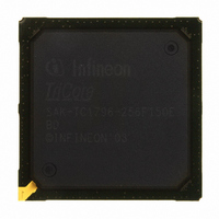
SAK-TC1796-256F150E BD Infineon Technologies, SAK-TC1796-256F150E BD Datasheet - Page 40

SAK-TC1796-256F150E BD
Manufacturer Part Number
SAK-TC1796-256F150E BD
Description
IC MCU 32BIT FLASH PG-BGA-416
Manufacturer
Infineon Technologies
Series
TC17xxr
Datasheet
1.SAK-TC1796-256F150E_BE.pdf
(134 pages)
Specifications of SAK-TC1796-256F150E BD
Core Processor
TriCore
Core Size
32-Bit
Speed
150MHz
Connectivity
ASC, CAN, EBI/EMI, MLI, MSC, SSC
Peripherals
DMA, POR, WDT
Number Of I /o
123
Program Memory Size
2MB (2M x 8)
Program Memory Type
FLASH
Ram Size
256K x 8
Voltage - Supply (vcc/vdd)
1.42 V ~ 1.58 V
Data Converters
A/D 44x12b
Oscillator Type
External
Operating Temperature
-40°C ~ 125°C
Package / Case
416-BGA
Packages
PG-BGA-416
Max Clock Frequency
150.0 MHz
Sram (incl. Cache)
256.0 KByte
Can Nodes
4
A / D Input Lines (incl. Fadc)
44
Program Memory
2.0 MB
For Use With
B158-H8537-G2-X-7600IN - KIT STARTER TC179X FAMILY
Lead Free Status / RoHS Status
Lead free / RoHS Compliant
Eeprom Size
-
Other names
KT1796256F150EBDXP
SAK-TC1796-256F150EBDIN
SP000228336
SAK-TC1796-256F150EBDIN
SP000228336
- Current page: 40 of 134
- Download datasheet (5Mb)
TC1796
Functional Description
3.4
Memory Protection System
The TC1796 memory protection system specifies the addressable range and read/write
permissions of memory segments available to the currently executing task. The memory
protection system controls the position and range of addressable segments in memory.
It also controls the kinds of read and write operations allowed within addressable
memory segments. Any illegal memory access is detected by the memory protection
hardware, which then invokes the appropriate Trap Service Routine (TSR) to handle the
error. Thus, the memory protection system protects critical system functions against both
software and hardware errors. The memory protection hardware can also generate
signals to the Debug Unit to facilitate tracing illegal memory accesses.
There are two Memory Protection Register Sets in the TC1796, numbered 0 and 1,
which specify memory protection ranges and permissions for code and data. The
PSW.PRS bit field determines which of these is the set currently in use by the CPU.
Because the TC1796 uses a Harvard-style memory architecture, each Memory
Protection Register Set is broken down into a Data Protection Register Set and a Code
Protection Register Set. Each Data Protection Register Set can specify up to four
address ranges to receive particular protection modes. Each Code Protection Register
Set can specify up to two address ranges to receive particular protection modes.
Each of the Data Protection Register Sets and Code Protection Register Sets
determines the range and protection modes for a separate memory area. Each contains
register pairs which determine the address range (the Data Segment Protection
Registers and Code Segment Protection Registers) and one register (Data Protection
Mode Register) which determines the memory access modes which apply to the
specified range.
Data Sheet
40
V1.0, 2008-04
Related parts for SAK-TC1796-256F150E BD
Image
Part Number
Description
Manufacturer
Datasheet
Request
R

Part Number:
Description:
IC MCU 32BIT FLASH 416-BGA
Manufacturer:
Infineon Technologies
Datasheet:

Part Number:
Description:
IC MCU 32BIT FLASH BGA-416
Manufacturer:
Infineon Technologies
Datasheet:

Part Number:
Description:
Manufacturer:
Infineon Technologies AG
Datasheet:

Part Number:
Description:
BGA 416/32 BIT FLASH
Manufacturer:
Infineon Technologies AG
Datasheet:

Part Number:
Description:
Manufacturer:
Infineon Technologies AG
Datasheet:

Part Number:
Description:
Manufacturer:
Infineon Technologies AG
Datasheet:

Part Number:
Description:
Manufacturer:
Infineon Technologies AG
Datasheet:

Part Number:
Description:
Manufacturer:
Infineon Technologies AG
Datasheet:

Part Number:
Description:
Manufacturer:
Infineon Technologies AG
Datasheet:

Part Number:
Description:
Manufacturer:
Infineon Technologies AG
Datasheet:

Part Number:
Description:
Manufacturer:
Infineon Technologies AG
Datasheet:

Part Number:
Description:
16-bit microcontroller with 2x2 KByte RAM
Manufacturer:
Infineon Technologies AG
Datasheet:

Part Number:
Description:
NPN silicon RF transistor
Manufacturer:
Infineon Technologies AG
Datasheet:

Part Number:
Description:
NPN silicon RF transistor
Manufacturer:
Infineon Technologies AG
Datasheet:

Part Number:
Description:
NPN silicon RF transistor
Manufacturer:
Infineon Technologies AG
Datasheet:


