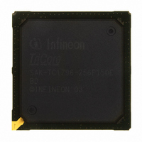
SAK-TC1796-256F150E BD Infineon Technologies, SAK-TC1796-256F150E BD Datasheet - Page 78

SAK-TC1796-256F150E BD
Manufacturer Part Number
SAK-TC1796-256F150E BD
Description
IC MCU 32BIT FLASH PG-BGA-416
Manufacturer
Infineon Technologies
Series
TC17xxr
Datasheet
1.SAK-TC1796-256F150E_BE.pdf
(134 pages)
Specifications of SAK-TC1796-256F150E BD
Core Processor
TriCore
Core Size
32-Bit
Speed
150MHz
Connectivity
ASC, CAN, EBI/EMI, MLI, MSC, SSC
Peripherals
DMA, POR, WDT
Number Of I /o
123
Program Memory Size
2MB (2M x 8)
Program Memory Type
FLASH
Ram Size
256K x 8
Voltage - Supply (vcc/vdd)
1.42 V ~ 1.58 V
Data Converters
A/D 44x12b
Oscillator Type
External
Operating Temperature
-40°C ~ 125°C
Package / Case
416-BGA
Packages
PG-BGA-416
Max Clock Frequency
150.0 MHz
Sram (incl. Cache)
256.0 KByte
Can Nodes
4
A / D Input Lines (incl. Fadc)
44
Program Memory
2.0 MB
For Use With
B158-H8537-G2-X-7600IN - KIT STARTER TC179X FAMILY
Lead Free Status / RoHS Status
Lead free / RoHS Compliant
Eeprom Size
-
Other names
KT1796256F150EBDXP
SAK-TC1796-256F150EBDIN
SP000228336
SAK-TC1796-256F150EBDIN
SP000228336
- Current page: 78 of 134
- Download datasheet (5Mb)
optimized together with the crystal vendor using the negative resistance method.
Oscillation measurement with the final target system is strongly recommended to verify
the input amplitude at XTAL1 and to determine the actual oscillation allowance (margin
negative resistance) for the oscillator-crystal system.
When using an external clock signal, it must be connected to XTAL1. XTAL2 is left open
(unconnected). The external clock frequency can be in the range of 0 - 40 MHz if the PLL
is bypassed and 4 - 40 MHz if the PLL is used.
The oscillator can also be used in combination with a ceramic resonator. The final
circuitry must be also verified by the resonator vendor.
Figure 20
modes, external crystal mode and external input clock mode.
Figure 20
A block capacitor between
Note: For crystal operation, it is strongly recommended to measure the negative
1)
Data Sheet
V
in future steps and products is kept open.
DDOSC
4 - 25
Fundamental
Mode Crystal
Crystal Frequency
4 MHz
8 MHz
12 MHz
16 - 25 MHz
1) Note that these are evaluation start values!
MHz
resistance in the final target system (layout) to determine the optimum parameters
C
X1
R
and
Q
shows the recommended external oscillator circuitries for both operating
V
SSOSC
Oscillator Circuitries
C
R
X2
X2
are not bonded externally in the BC and BD steps of TC1796. An option for bonding them
V
XTAL1
XTAL2
DDOSC
C
33 pF
18 pF
12 pF
10 pF
Oscillator
X1
TC1796
V
,
SSOSC
C
X2
V
V
DDOSC
1)
DDOSC3
R
0
0
0
0
1)
X2
/
V
f
1)
OSC
DDOSC3
78
and
External Clock
Signal
1) in case of PLL bypass 0 MHz
V
SSOSC
4
1)
is recommended, too.
MHz
- 40
Functional Description
V
XTAL1
XTAL2
DDOSC
Oscillator
TC1796
V
SSOSC
V
DDOSC3
V1.0, 2008-04
MCS05601
TC1796
f
OSC
Related parts for SAK-TC1796-256F150E BD
Image
Part Number
Description
Manufacturer
Datasheet
Request
R

Part Number:
Description:
IC MCU 32BIT FLASH 416-BGA
Manufacturer:
Infineon Technologies
Datasheet:

Part Number:
Description:
IC MCU 32BIT FLASH BGA-416
Manufacturer:
Infineon Technologies
Datasheet:

Part Number:
Description:
Manufacturer:
Infineon Technologies AG
Datasheet:

Part Number:
Description:
BGA 416/32 BIT FLASH
Manufacturer:
Infineon Technologies AG
Datasheet:

Part Number:
Description:
Manufacturer:
Infineon Technologies AG
Datasheet:

Part Number:
Description:
Manufacturer:
Infineon Technologies AG
Datasheet:

Part Number:
Description:
Manufacturer:
Infineon Technologies AG
Datasheet:

Part Number:
Description:
Manufacturer:
Infineon Technologies AG
Datasheet:

Part Number:
Description:
Manufacturer:
Infineon Technologies AG
Datasheet:

Part Number:
Description:
Manufacturer:
Infineon Technologies AG
Datasheet:

Part Number:
Description:
Manufacturer:
Infineon Technologies AG
Datasheet:

Part Number:
Description:
16-bit microcontroller with 2x2 KByte RAM
Manufacturer:
Infineon Technologies AG
Datasheet:

Part Number:
Description:
NPN silicon RF transistor
Manufacturer:
Infineon Technologies AG
Datasheet:

Part Number:
Description:
NPN silicon RF transistor
Manufacturer:
Infineon Technologies AG
Datasheet:

Part Number:
Description:
NPN silicon RF transistor
Manufacturer:
Infineon Technologies AG
Datasheet:


