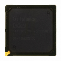
SAK-TC1796-256F150E BD Infineon Technologies, SAK-TC1796-256F150E BD Datasheet - Page 31

SAK-TC1796-256F150E BD
Manufacturer Part Number
SAK-TC1796-256F150E BD
Description
IC MCU 32BIT FLASH PG-BGA-416
Manufacturer
Infineon Technologies
Series
TC17xxr
Datasheet
1.SAK-TC1796-256F150E_BE.pdf
(134 pages)
Specifications of SAK-TC1796-256F150E BD
Core Processor
TriCore
Core Size
32-Bit
Speed
150MHz
Connectivity
ASC, CAN, EBI/EMI, MLI, MSC, SSC
Peripherals
DMA, POR, WDT
Number Of I /o
123
Program Memory Size
2MB (2M x 8)
Program Memory Type
FLASH
Ram Size
256K x 8
Voltage - Supply (vcc/vdd)
1.42 V ~ 1.58 V
Data Converters
A/D 44x12b
Oscillator Type
External
Operating Temperature
-40°C ~ 125°C
Package / Case
416-BGA
Packages
PG-BGA-416
Max Clock Frequency
150.0 MHz
Sram (incl. Cache)
256.0 KByte
Can Nodes
4
A / D Input Lines (incl. Fadc)
44
Program Memory
2.0 MB
For Use With
B158-H8537-G2-X-7600IN - KIT STARTER TC179X FAMILY
Lead Free Status / RoHS Status
Lead free / RoHS Compliant
Eeprom Size
-
Other names
KT1796256F150EBDXP
SAK-TC1796-256F150EBDIN
SP000228336
SAK-TC1796-256F150EBDIN
SP000228336
- Current page: 31 of 134
- Download datasheet (5Mb)
Table 2
Symbol
System I/O
TRST
TCK
TDI
TDO
TMS
BRKIN
BRK
OUT
NMI
HDRST
PORST
BYPASS A24
TEST
MODE
TSTRES G24
Data Sheet
Pins
F23
E24
E25
D25
F24
C26
D26
A22
A23
B22
B23
Pin Definitions and Functions (cont’d)
I/O Pad
I
I
I
O
I
I/O A3
I/O A3
I
I/O A2
I
I
I
I
Class
A2
A2
A1
A2
A1
–
–
A1
–
–
Power
Supply
V
DDP
31
Functions
JTAG Module Reset/Enable Input
JTAG Module Clock Input
JTAG Module Serial Data Input
JTAG Module Serial Data Output
JTAG Module State Machine Control
Input
OCDS Break Input (Alternate Output)
OCDS Break Output (Alternate Input)
Non-Maskable Interrupt Input
(input pad with input spike-filter.)
Hardware Reset Input / Reset Indication
Output
(open drain pad with input spike-filter.)
Power-on Reset Input
(input pad with input spike-filter.)
PLL Bypass Select Input
This input has to be held stable between to
power-on resets. With BYPASS = 1 the
spike filters in the HDRST, PORST, and
NMI inputs are switched off.
Test Mode Select Input
For normal operation of the TC1796, this
pin should be connected to high level.
(input pad, test function only, without input
spike-filter.)
Test Reset Input
For normal operation of the TC1796, this
pin should be connected to low level.
Otherwise an unpredictable reset behavior
may occur.
(input pad, test function only, without input
spike-filter.)
General Device Information
2)
V1.0, 2008-04
TC1796
2)
2)
2)
Related parts for SAK-TC1796-256F150E BD
Image
Part Number
Description
Manufacturer
Datasheet
Request
R

Part Number:
Description:
IC MCU 32BIT FLASH 416-BGA
Manufacturer:
Infineon Technologies
Datasheet:

Part Number:
Description:
IC MCU 32BIT FLASH BGA-416
Manufacturer:
Infineon Technologies
Datasheet:

Part Number:
Description:
Manufacturer:
Infineon Technologies AG
Datasheet:

Part Number:
Description:
BGA 416/32 BIT FLASH
Manufacturer:
Infineon Technologies AG
Datasheet:

Part Number:
Description:
Manufacturer:
Infineon Technologies AG
Datasheet:

Part Number:
Description:
Manufacturer:
Infineon Technologies AG
Datasheet:

Part Number:
Description:
Manufacturer:
Infineon Technologies AG
Datasheet:

Part Number:
Description:
Manufacturer:
Infineon Technologies AG
Datasheet:

Part Number:
Description:
Manufacturer:
Infineon Technologies AG
Datasheet:

Part Number:
Description:
Manufacturer:
Infineon Technologies AG
Datasheet:

Part Number:
Description:
Manufacturer:
Infineon Technologies AG
Datasheet:

Part Number:
Description:
16-bit microcontroller with 2x2 KByte RAM
Manufacturer:
Infineon Technologies AG
Datasheet:

Part Number:
Description:
NPN silicon RF transistor
Manufacturer:
Infineon Technologies AG
Datasheet:

Part Number:
Description:
NPN silicon RF transistor
Manufacturer:
Infineon Technologies AG
Datasheet:

Part Number:
Description:
NPN silicon RF transistor
Manufacturer:
Infineon Technologies AG
Datasheet:


