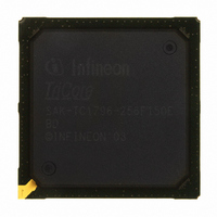
SAK-TC1796-256F150E BD Infineon Technologies, SAK-TC1796-256F150E BD Datasheet - Page 107

SAK-TC1796-256F150E BD
Manufacturer Part Number
SAK-TC1796-256F150E BD
Description
IC MCU 32BIT FLASH PG-BGA-416
Manufacturer
Infineon Technologies
Series
TC17xxr
Datasheet
1.SAK-TC1796-256F150E_BE.pdf
(134 pages)
Specifications of SAK-TC1796-256F150E BD
Core Processor
TriCore
Core Size
32-Bit
Speed
150MHz
Connectivity
ASC, CAN, EBI/EMI, MLI, MSC, SSC
Peripherals
DMA, POR, WDT
Number Of I /o
123
Program Memory Size
2MB (2M x 8)
Program Memory Type
FLASH
Ram Size
256K x 8
Voltage - Supply (vcc/vdd)
1.42 V ~ 1.58 V
Data Converters
A/D 44x12b
Oscillator Type
External
Operating Temperature
-40°C ~ 125°C
Package / Case
416-BGA
Packages
PG-BGA-416
Max Clock Frequency
150.0 MHz
Sram (incl. Cache)
256.0 KByte
Can Nodes
4
A / D Input Lines (incl. Fadc)
44
Program Memory
2.0 MB
For Use With
B158-H8537-G2-X-7600IN - KIT STARTER TC179X FAMILY
Lead Free Status / RoHS Status
Lead free / RoHS Compliant
Eeprom Size
-
Other names
KT1796256F150EBDXP
SAK-TC1796-256F150EBDIN
SP000228336
SAK-TC1796-256F150EBDIN
SP000228336
- Current page: 107 of 134
- Download datasheet (5Mb)
2) Parameter test correlation for
4.3.3
There is a restriction for the power sequencing of the 3.3 V domain including
shown in
shows the valid range for
V
referenced in
anti parallel ESD protection diodes in TC1796 design steps BC and BD. The
V
diodes in TC1796 design step BE.
V
V
Figure 29
All ground pins
The difference voltage between the ground pins must not exceed 200 mV.
The PORST signal must be activated at latest before any power supply voltage falls
below the levels shown on the figure below. In this case, only the memory row of a Flash
memory that was a target of a write at the moment of the power loss will contain
unreliable content. Additionally, the PORST signal should be activated as soon as
possible. The sooner the PORST signal is activated, the less time the system operates
outside of the normal operating power supply range.
Data Sheet
DDP
DDMF
DD
DDEBU
,
,
V
,
V
DDOSC
belongs to its own 2.5V to 3.3V domain.
V
DDOSC3
DDP
Figure
Power Sequencing
,
and
(3.3V)
Figure 29
V
,
V
V
3.3V
1.5V
V
V
DDOSC3
DDP
DDP
SS
29: it must always be higher than 1.5 V domain - 0.5 V. The grey area
DDFL3
V
DDAF
/
must be externally connected to one single star point in the system.
V
,
DDEBU
PORST
sub domains are connected with anti parallel ESD protection
belong to the 1.5 V power supply domain, referenced as
V
as
DDM
V
V
DDEBU
3.3V
V
,
/
3.3
V
V
and
. The
DDMF
DD
= 2.5 V ± 5%
V
3.3
Power Up Sequence
V
, V
belong to the 3.3 V power supply domain, that is
DDEBU
V
DDEBU
DDM
107
> V
relative to an exemplary 1.5 V ramp.
and
1.5
- 0.5V
V
DDMF
sub domains are connected with
V
V
1.5
3.3
, V
Electrical Parameters
DDEBU
PowerSeq 2
Time
Time
V1.0, 2008-04
V
TC1796
DDEBU
V
V
1.5
DDM
.
as
,
Related parts for SAK-TC1796-256F150E BD
Image
Part Number
Description
Manufacturer
Datasheet
Request
R

Part Number:
Description:
IC MCU 32BIT FLASH 416-BGA
Manufacturer:
Infineon Technologies
Datasheet:

Part Number:
Description:
IC MCU 32BIT FLASH BGA-416
Manufacturer:
Infineon Technologies
Datasheet:

Part Number:
Description:
Manufacturer:
Infineon Technologies AG
Datasheet:

Part Number:
Description:
BGA 416/32 BIT FLASH
Manufacturer:
Infineon Technologies AG
Datasheet:

Part Number:
Description:
Manufacturer:
Infineon Technologies AG
Datasheet:

Part Number:
Description:
Manufacturer:
Infineon Technologies AG
Datasheet:

Part Number:
Description:
Manufacturer:
Infineon Technologies AG
Datasheet:

Part Number:
Description:
Manufacturer:
Infineon Technologies AG
Datasheet:

Part Number:
Description:
Manufacturer:
Infineon Technologies AG
Datasheet:

Part Number:
Description:
Manufacturer:
Infineon Technologies AG
Datasheet:

Part Number:
Description:
Manufacturer:
Infineon Technologies AG
Datasheet:

Part Number:
Description:
16-bit microcontroller with 2x2 KByte RAM
Manufacturer:
Infineon Technologies AG
Datasheet:

Part Number:
Description:
NPN silicon RF transistor
Manufacturer:
Infineon Technologies AG
Datasheet:

Part Number:
Description:
NPN silicon RF transistor
Manufacturer:
Infineon Technologies AG
Datasheet:

Part Number:
Description:
NPN silicon RF transistor
Manufacturer:
Infineon Technologies AG
Datasheet:


