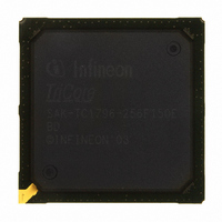
SAK-TC1796-256F150E BD Infineon Technologies, SAK-TC1796-256F150E BD Datasheet - Page 84

SAK-TC1796-256F150E BD
Manufacturer Part Number
SAK-TC1796-256F150E BD
Description
IC MCU 32BIT FLASH PG-BGA-416
Manufacturer
Infineon Technologies
Series
TC17xxr
Datasheet
1.SAK-TC1796-256F150E_BE.pdf
(134 pages)
Specifications of SAK-TC1796-256F150E BD
Core Processor
TriCore
Core Size
32-Bit
Speed
150MHz
Connectivity
ASC, CAN, EBI/EMI, MLI, MSC, SSC
Peripherals
DMA, POR, WDT
Number Of I /o
123
Program Memory Size
2MB (2M x 8)
Program Memory Type
FLASH
Ram Size
256K x 8
Voltage - Supply (vcc/vdd)
1.42 V ~ 1.58 V
Data Converters
A/D 44x12b
Oscillator Type
External
Operating Temperature
-40°C ~ 125°C
Package / Case
416-BGA
Packages
PG-BGA-416
Max Clock Frequency
150.0 MHz
Sram (incl. Cache)
256.0 KByte
Can Nodes
4
A / D Input Lines (incl. Fadc)
44
Program Memory
2.0 MB
For Use With
B158-H8537-G2-X-7600IN - KIT STARTER TC179X FAMILY
Lead Free Status / RoHS Status
Lead free / RoHS Compliant
Eeprom Size
-
Other names
KT1796256F150EBDXP
SAK-TC1796-256F150EBDIN
SP000228336
SAK-TC1796-256F150EBDIN
SP000228336
4.1.3
Stresses above those listed under “Absolute Maximum Ratings” may cause permanent
damage to the device. This is a stress rating only and functional operation of the device
at these or any other conditions above those indicated in the operational sections of this
specification is not implied. Exposure to absolute maximum rating conditions for
extended periods may affect device reliability.
During absolute maximum rating overload conditions (
voltage on the related
defined by the absolute maximum ratings.
Table 11
Parameter
Ambient temperature
Storage temperature
Junction temperature
Voltage at 1.5 V power supply
pins with respect to
Voltage at 3.3 V power supply
pins with respect to
Voltage on any Class A input
pin and dedicated input pins
with respect to
Voltage on any Class B input
pin with respect to
Voltage on any Class D
analog input pin with respect
to
Voltage on any Class D
analog input pin with respect
to
CPU & LMB Bus Frequency
FPI Bus Frequency
1) Applicable for
2) Applicable for
3) The PLL jitter characteristics add to this value according to the application settings. See the PLL jitter
Data Sheet
V
V
parameters.
AGND
SSAF
Absolute Maximum Ratings
V
V
Absolute Maximum Rating Parameters
DD
DDP
V
SS
,
,
V
V
V
DDSBRAM
DDEBU
V
V
SS
SS
SS
V
1)
2)
DD
,
,
V
V
DDFL3,
pins with respect to ground (
DDOSC
V
Symbol
T
T
T
V
V
V
V
V
V
V
V
V
f
f
,
CPU
SYS
DDM
V
A
ST
J
DD
DDEBU
DDP
IN
IN
AIN
AREFx
AINF
FAREF
DDPLL
, and
, and
SR -40
SR -0.5 –
SR
SR
SR
SR –
SR -65
SR -0.5 –
SR –
SR -40
SR
V
DDMF
V
84
Min. Typ. Max.
–
–
-0.5 –
-0.5 –
DDAF
.
.
–
–
–
–
–
–
–
Values
V
V
IN
125
150
150
2.25
3.75
V
or max. 3.7
V
or max. 3.7
V
or
max. 3.7
V
or
max. 3.7
150
75
SS
DDP
DDEBU
DDM
DDMF
> related
3)
) must not exceed the values
3)
+ 0.5
+ 0.5
+ 0.5
+ 0.5
Electrical Parameters
V
DD
Unit Note /
°C
°C
°C
V
V
V
V
V
V
MHz –
MHz –
or
V
V1.0, 2008-04
IN
Test Con
dition
Under bias
–
Under bias
–
–
Whatever
is lower
Whatever
is lower
Whatever
is lower
Whatever
is lower
<
TC1796
V
SS
) the


