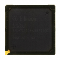
SAK-TC1796-256F150E BD Infineon Technologies, SAK-TC1796-256F150E BD Datasheet - Page 110

SAK-TC1796-256F150E BD
Manufacturer Part Number
SAK-TC1796-256F150E BD
Description
IC MCU 32BIT FLASH PG-BGA-416
Manufacturer
Infineon Technologies
Series
TC17xxr
Datasheet
1.SAK-TC1796-256F150E_BE.pdf
(134 pages)
Specifications of SAK-TC1796-256F150E BD
Core Processor
TriCore
Core Size
32-Bit
Speed
150MHz
Connectivity
ASC, CAN, EBI/EMI, MLI, MSC, SSC
Peripherals
DMA, POR, WDT
Number Of I /o
123
Program Memory Size
2MB (2M x 8)
Program Memory Type
FLASH
Ram Size
256K x 8
Voltage - Supply (vcc/vdd)
1.42 V ~ 1.58 V
Data Converters
A/D 44x12b
Oscillator Type
External
Operating Temperature
-40°C ~ 125°C
Package / Case
416-BGA
Packages
PG-BGA-416
Max Clock Frequency
150.0 MHz
Sram (incl. Cache)
256.0 KByte
Can Nodes
4
A / D Input Lines (incl. Fadc)
44
Program Memory
2.0 MB
For Use With
B158-H8537-G2-X-7600IN - KIT STARTER TC179X FAMILY
Lead Free Status / RoHS Status
Lead free / RoHS Compliant
Eeprom Size
-
Other names
KT1796256F150EBDXP
SAK-TC1796-256F150EBDIN
SP000228336
SAK-TC1796-256F150EBDIN
SP000228336
- Current page: 110 of 134
- Download datasheet (5Mb)
1) This parameter is valid under assumption that PORST signal is constantly at low level during the power-
2)
3) Any HDRST activation is internally prolonged to 1024 FPI bus clock (
4) Applicable for input pins TESTMODE, TRST, BRKIN, and TXD1A with noise suppression filter of PORST
5) The setup/hold values are applicable for Port 0 and Port 10 input pins with noise suppression filter of HDRST
6)
7) Not subject to production test, verified by design / characterization.
8) This parameter includes the delay of the analog spike filter in the PORST pad.
9) The duration of the boot-time is defined between the rising edge of the PORST and the moment when the first
10) The duration of the boot time is defined between the following events:
Data Sheet
up/power-down of the
t
0,3*
optimized by the customer and checked for negative resistance as recommended and specified by crystal
suppliers.
switched-on (BYPASS = 0).
switched-on (BYPASS = 0), independently whether HDRST is used as input or output.
f
user instruction has entered the CPU and its processing starts.
1. Hardware reset: the falling edge of a short HDRST pulse and the moment when the first user instruction
has entered the CPU and its processing starts, if the HDRST pulse is shorter than 1024 ×
If the HDRST pulse is longer than 1024 ×
boot time (HDRST falling edge to first user instruction).
2. Software reset: the moment of starting the software reset and the moment when the first user instruction
has entered the CPU and its processing starts
OSCS
SYS
V
=
DDOSC3
is defined from the moment when
f
CPU
/2
. This parameter is verified by device characterization. The external oscillator circuitry must be
V
DDP
.
V
DDOSC3
T
SYS
, only the time beyond the 1024 ×
= 3.13V until the oscillations reach an amplitude at XTAL1 of
110
f
SYS
) cycles.
Electrical Parameters
T
SYS
should be added to the
T
SYS
V1.0, 2008-04
.
TC1796
Related parts for SAK-TC1796-256F150E BD
Image
Part Number
Description
Manufacturer
Datasheet
Request
R

Part Number:
Description:
IC MCU 32BIT FLASH 416-BGA
Manufacturer:
Infineon Technologies
Datasheet:

Part Number:
Description:
IC MCU 32BIT FLASH BGA-416
Manufacturer:
Infineon Technologies
Datasheet:

Part Number:
Description:
Manufacturer:
Infineon Technologies AG
Datasheet:

Part Number:
Description:
BGA 416/32 BIT FLASH
Manufacturer:
Infineon Technologies AG
Datasheet:

Part Number:
Description:
Manufacturer:
Infineon Technologies AG
Datasheet:

Part Number:
Description:
Manufacturer:
Infineon Technologies AG
Datasheet:

Part Number:
Description:
Manufacturer:
Infineon Technologies AG
Datasheet:

Part Number:
Description:
Manufacturer:
Infineon Technologies AG
Datasheet:

Part Number:
Description:
Manufacturer:
Infineon Technologies AG
Datasheet:

Part Number:
Description:
Manufacturer:
Infineon Technologies AG
Datasheet:

Part Number:
Description:
Manufacturer:
Infineon Technologies AG
Datasheet:

Part Number:
Description:
16-bit microcontroller with 2x2 KByte RAM
Manufacturer:
Infineon Technologies AG
Datasheet:

Part Number:
Description:
NPN silicon RF transistor
Manufacturer:
Infineon Technologies AG
Datasheet:

Part Number:
Description:
NPN silicon RF transistor
Manufacturer:
Infineon Technologies AG
Datasheet:

Part Number:
Description:
NPN silicon RF transistor
Manufacturer:
Infineon Technologies AG
Datasheet:


