SAK-TC1796-256F150E BD Infineon Technologies, SAK-TC1796-256F150E BD Datasheet - Page 36
SAK-TC1796-256F150E BD
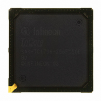
Manufacturer Part Number
SAK-TC1796-256F150E BD
Description
IC MCU 32BIT FLASH PG-BGA-416
Manufacturer
Infineon Technologies
Series
TC17xxr
Datasheet
1.SAK-TC1796-256F150E_BE.pdf
(134 pages)
Specifications of SAK-TC1796-256F150E BD
Core Processor
TriCore
Core Size
32-Bit
Speed
150MHz
Connectivity
ASC, CAN, EBI/EMI, MLI, MSC, SSC
Peripherals
DMA, POR, WDT
Number Of I /o
123
Program Memory Size
2MB (2M x 8)
Program Memory Type
FLASH
Ram Size
256K x 8
Voltage - Supply (vcc/vdd)
1.42 V ~ 1.58 V
Data Converters
A/D 44x12b
Oscillator Type
External
Operating Temperature
-40°C ~ 125°C
Package / Case
416-BGA
Packages
PG-BGA-416
Max Clock Frequency
150.0 MHz
Sram (incl. Cache)
256.0 KByte
Can Nodes
4
A / D Input Lines (incl. Fadc)
44
Program Memory
2.0 MB
For Use With
B158-H8537-G2-X-7600IN - KIT STARTER TC179X FAMILY
Lead Free Status / RoHS Status
Lead free / RoHS Compliant
Eeprom Size
-
Other names
KT1796256F150EBDXP
SAK-TC1796-256F150EBDIN
SP000228336
SAK-TC1796-256F150EBDIN
SP000228336


3
The following section gives an overview of the sub systems and the modules of the
TC1796 and their connectivity.
3.1
The TC1796 has four independent on-chip buses (see also TC1796 block diagram in
Figure
•
•
•
•
The two LMB Buses (Program Local Memory Bus PLMB and Data Local Memory Bus
DLMB) connect the TriCore CPU to its local resources for data and instruction fetches.
The PLMB/DLMB Buses are synchronous and pipelined buses with variable block size
transfer support. The protocol supports 8-, 16-, 32-, and 64-bit single transactions and
variable length 64-bit block transfers.
The System Peripheral Bus (SPB) is accessible by the CPU via the LFI Bridge. The
LFI Bridge is a bi-directional bus bridge between the DLMB and the SPB. It supports all
transactions types of both buses, DLMB Bus and FPI Bus. It handles address translation
and transaction type translation between the two buses. The LFI Bridge further supports
the pipelining of both connected buses. Therefore, no additional delay is created except
for bus protocol conversions.
The Remote Peripheral Bus (RPB) connects the peripherals with high data rates (SSC,
ADC, FADC) with the Dual-port memory (DPRAM) in the DMI, relieving the SPB and the
PLMB/DLMB Buses from these data transfers. The RPB is controlled by a bus switch
which is located in the DMA controller.
The two LMB Buses are running at CPU clock speed (clock rate of
RPB are running at system clock speed (clock rate of
to
Data Sheet
f
CPU
Program Local Memory Bus (PLMB)
Data Local Memory Bus (DLMB)
System Peripheral Bus (SPB)
Remote Peripheral Bus (RPB)
or half the
1):
Functional Description
System Architecture and On-Chip Bus Systems
f
CPU
frequency.
36
f
SYS
). Note that
Functional Description
f
CPU
f
SYS
) while SPB and
can be equal
V1.0, 2008-04
TC1796
Related parts for SAK-TC1796-256F150E BD
Image
Part Number
Description
Manufacturer
Datasheet
Request
R

Part Number:
Description:
IC MCU 32BIT FLASH 416-BGA
Manufacturer:
Infineon Technologies
Datasheet:
Part Number:
Description:
IC MCU 32BIT FLASH BGA-416
Manufacturer:
Infineon Technologies
Datasheet:

Part Number:
Description:
Manufacturer:
Infineon Technologies AG
Datasheet:
Part Number:
Description:
BGA 416/32 BIT FLASH
Manufacturer:
Infineon Technologies AG
Datasheet:
Part Number:
Description:
Manufacturer:
Infineon Technologies AG
Datasheet:
Part Number:
Description:
Manufacturer:
Infineon Technologies AG
Datasheet:
Part Number:
Description:
Manufacturer:
Infineon Technologies AG
Datasheet:
Part Number:
Description:
Manufacturer:
Infineon Technologies AG
Datasheet:
Part Number:
Description:
Manufacturer:
Infineon Technologies AG
Datasheet:
Part Number:
Description:
Manufacturer:
Infineon Technologies AG
Datasheet:
Part Number:
Description:
Manufacturer:
Infineon Technologies AG
Datasheet:
Part Number:
Description:
16-bit microcontroller with 2x2 KByte RAM
Manufacturer:
Infineon Technologies AG
Datasheet:
Part Number:
Description:
NPN silicon RF transistor
Manufacturer:
Infineon Technologies AG
Datasheet:
Part Number:
Description:
NPN silicon RF transistor
Manufacturer:
Infineon Technologies AG
Datasheet:
Part Number:
Description:
NPN silicon RF transistor
Manufacturer:
Infineon Technologies AG
Datasheet: