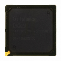
SAK-TC1796-256F150E BD Infineon Technologies, SAK-TC1796-256F150E BD Datasheet - Page 66

SAK-TC1796-256F150E BD
Manufacturer Part Number
SAK-TC1796-256F150E BD
Description
IC MCU 32BIT FLASH PG-BGA-416
Manufacturer
Infineon Technologies
Series
TC17xxr
Datasheet
1.SAK-TC1796-256F150E_BE.pdf
(134 pages)
Specifications of SAK-TC1796-256F150E BD
Core Processor
TriCore
Core Size
32-Bit
Speed
150MHz
Connectivity
ASC, CAN, EBI/EMI, MLI, MSC, SSC
Peripherals
DMA, POR, WDT
Number Of I /o
123
Program Memory Size
2MB (2M x 8)
Program Memory Type
FLASH
Ram Size
256K x 8
Voltage - Supply (vcc/vdd)
1.42 V ~ 1.58 V
Data Converters
A/D 44x12b
Oscillator Type
External
Operating Temperature
-40°C ~ 125°C
Package / Case
416-BGA
Packages
PG-BGA-416
Max Clock Frequency
150.0 MHz
Sram (incl. Cache)
256.0 KByte
Can Nodes
4
A / D Input Lines (incl. Fadc)
44
Program Memory
2.0 MB
For Use With
B158-H8537-G2-X-7600IN - KIT STARTER TC179X FAMILY
Lead Free Status / RoHS Status
Lead free / RoHS Compliant
Eeprom Size
-
Other names
KT1796256F150EBDXP
SAK-TC1796-256F150EBDIN
SP000228336
SAK-TC1796-256F150EBDIN
SP000228336
- Current page: 66 of 134
- Download datasheet (5Mb)
Figure 16
Features
•
•
•
•
•
•
•
•
•
•
•
Data Sheet
Extreme fast conversion: 21 cycles of
10-bit A/D conversion
– Higher resolution by averaging of consecutive conversions is supported
Successive approximation conversion method
Four differential input channels
Offset and gain calibration support for each channel
Differential input amplifier with programmable gain of 1, 2, 4 and 8 for each channel
Free-running (Channel Timers) or triggered conversion modes
Trigger and gating control for external signals
Built-in Channel Timers for internal triggering
Channel timer request periods independently selectable for each channel
Selectable, programmable anti aliasing and data reduction filter block
Address
Decoder
Interrupt
To DMA
Control
Control
GPTA0
External Request Unit
Clock
Block Diagram of the FADC Module
(SCU)
OUT1
OUT9
OUT18
OUT26
OUT2
OUT10
OUT19
OUT27
SR[3:0]
f
FADC
f
CLC
PDOUT2
PDOUT3
V
FAREF
V
FAGND
V
Module
GS[7:0]
DDAF
TS[7:0]
Kernel
FADC
V
SSAF
f
FADC
66
V
DDMF
V
(= 280ns @
SSMF
FAIN0P
FAIN0N
FAIN1P
FAIN1N
FAIN2P
FAIN2N
FAIN3P
FAIN3N
f
FADC
Functional Description
= 75 MHz)
A1
A1
A1
A1
D
D
D
D
D
D
D
D
AN24
AN25
AN26
AN27
AN28
AN29
AN30
AN31
P1.0 / REQ0
P1.1 / REQ1
P7.0 / REQ4
P7.1 / REQ5
MCA06053
V1.0, 2008-04
TC1796
Related parts for SAK-TC1796-256F150E BD
Image
Part Number
Description
Manufacturer
Datasheet
Request
R

Part Number:
Description:
IC MCU 32BIT FLASH 416-BGA
Manufacturer:
Infineon Technologies
Datasheet:

Part Number:
Description:
IC MCU 32BIT FLASH BGA-416
Manufacturer:
Infineon Technologies
Datasheet:

Part Number:
Description:
Manufacturer:
Infineon Technologies AG
Datasheet:

Part Number:
Description:
BGA 416/32 BIT FLASH
Manufacturer:
Infineon Technologies AG
Datasheet:

Part Number:
Description:
Manufacturer:
Infineon Technologies AG
Datasheet:

Part Number:
Description:
Manufacturer:
Infineon Technologies AG
Datasheet:

Part Number:
Description:
Manufacturer:
Infineon Technologies AG
Datasheet:

Part Number:
Description:
Manufacturer:
Infineon Technologies AG
Datasheet:

Part Number:
Description:
Manufacturer:
Infineon Technologies AG
Datasheet:

Part Number:
Description:
Manufacturer:
Infineon Technologies AG
Datasheet:

Part Number:
Description:
Manufacturer:
Infineon Technologies AG
Datasheet:

Part Number:
Description:
16-bit microcontroller with 2x2 KByte RAM
Manufacturer:
Infineon Technologies AG
Datasheet:

Part Number:
Description:
NPN silicon RF transistor
Manufacturer:
Infineon Technologies AG
Datasheet:

Part Number:
Description:
NPN silicon RF transistor
Manufacturer:
Infineon Technologies AG
Datasheet:

Part Number:
Description:
NPN silicon RF transistor
Manufacturer:
Infineon Technologies AG
Datasheet:


