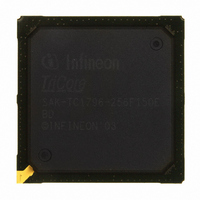
SAK-TC1796-256F150E BD Infineon Technologies, SAK-TC1796-256F150E BD Datasheet - Page 37

SAK-TC1796-256F150E BD
Manufacturer Part Number
SAK-TC1796-256F150E BD
Description
IC MCU 32BIT FLASH PG-BGA-416
Manufacturer
Infineon Technologies
Series
TC17xxr
Datasheet
1.SAK-TC1796-256F150E_BE.pdf
(134 pages)
Specifications of SAK-TC1796-256F150E BD
Core Processor
TriCore
Core Size
32-Bit
Speed
150MHz
Connectivity
ASC, CAN, EBI/EMI, MLI, MSC, SSC
Peripherals
DMA, POR, WDT
Number Of I /o
123
Program Memory Size
2MB (2M x 8)
Program Memory Type
FLASH
Ram Size
256K x 8
Voltage - Supply (vcc/vdd)
1.42 V ~ 1.58 V
Data Converters
A/D 44x12b
Oscillator Type
External
Operating Temperature
-40°C ~ 125°C
Package / Case
416-BGA
Packages
PG-BGA-416
Max Clock Frequency
150.0 MHz
Sram (incl. Cache)
256.0 KByte
Can Nodes
4
A / D Input Lines (incl. Fadc)
44
Program Memory
2.0 MB
For Use With
B158-H8537-G2-X-7600IN - KIT STARTER TC179X FAMILY
Lead Free Status / RoHS Status
Lead free / RoHS Compliant
Eeprom Size
-
Other names
KT1796256F150EBDXP
SAK-TC1796-256F150EBDIN
SP000228336
SAK-TC1796-256F150EBDIN
SP000228336
- Current page: 37 of 134
- Download datasheet (5Mb)
3.2
As shown in the TC1796 block diagram on
on-chip memories that are used as program or data memory.
•
•
•
•
Features of the Program Flash
•
•
•
•
•
•
•
•
•
•
•
•
Data Sheet
Program memory in PMU and PMI
– 2 Mbyte on-chip Program Flash (PFLASH)
– 16 Kbyte Boot ROM (BROM)
– 48 Kbyte Scratch-Pad RAM (SPRAM)
– 16 Kbyte Instruction Cache (ICACHE)
Data memory in DMU, PMU and DMI
– 56 Kbyte Local Data RAM (LDRAM)
– 8 Kbyte Dual-port RAM (DPRAM)
– 64 Kbyte Data Memory (SRAM)
– 16 Kbyte data memory (SBRAM) for standby operation during power-down
– 128 Kbyte on-chip Data Flash (DFLASH)
Memory of the PCP2
– 32 Kbyte Code Memory (CMEM)
– 16 Kbyte Parameter Memory (PRAM)
On-chip SRAMs with parity error detection
2 Mbyte on-chip program Flash memory
Usable for instruction code execution or constant data storage
256-byte wide program interface
– 256 bytes are programmed into PFLASH page in one step/command
256-bit read interface
– Transfer from PFLASH to CPU/PMI by four 64-bit single-cycle burst transfers
Dynamic correction of single-bit errors during read access
Detection of double bit errors
Fixed sector architecture
– Eight 16 Kbyte, one 128 Kbyte, one 256 Kbyte, and three 512 Kbyte sectors
– Each sector separately erasable
– Each sector separately write-protectable
Configurable read protection for complete PFLASH with sophisticated read access
supervision, combined with write protection for complete PFLASH (protection against
“Trojan horse” software)
Configurable write protection for each sector
– Each sector separately write-protectable
– With capability to be re-programmed
– With capability to be locked forever (OTP)
Password mechanism for temporarily disable write or read protection
On-chip programming voltage generation
PFLASH is delivered in erased state (read all zeros)
On-Chip Memories
37
Page
10, some of the TC1796 units provide
Functional Description
V1.0, 2008-04
TC1796
Related parts for SAK-TC1796-256F150E BD
Image
Part Number
Description
Manufacturer
Datasheet
Request
R

Part Number:
Description:
IC MCU 32BIT FLASH 416-BGA
Manufacturer:
Infineon Technologies
Datasheet:

Part Number:
Description:
IC MCU 32BIT FLASH BGA-416
Manufacturer:
Infineon Technologies
Datasheet:

Part Number:
Description:
Manufacturer:
Infineon Technologies AG
Datasheet:

Part Number:
Description:
BGA 416/32 BIT FLASH
Manufacturer:
Infineon Technologies AG
Datasheet:

Part Number:
Description:
Manufacturer:
Infineon Technologies AG
Datasheet:

Part Number:
Description:
Manufacturer:
Infineon Technologies AG
Datasheet:

Part Number:
Description:
Manufacturer:
Infineon Technologies AG
Datasheet:

Part Number:
Description:
Manufacturer:
Infineon Technologies AG
Datasheet:

Part Number:
Description:
Manufacturer:
Infineon Technologies AG
Datasheet:

Part Number:
Description:
Manufacturer:
Infineon Technologies AG
Datasheet:

Part Number:
Description:
Manufacturer:
Infineon Technologies AG
Datasheet:

Part Number:
Description:
16-bit microcontroller with 2x2 KByte RAM
Manufacturer:
Infineon Technologies AG
Datasheet:

Part Number:
Description:
NPN silicon RF transistor
Manufacturer:
Infineon Technologies AG
Datasheet:

Part Number:
Description:
NPN silicon RF transistor
Manufacturer:
Infineon Technologies AG
Datasheet:

Part Number:
Description:
NPN silicon RF transistor
Manufacturer:
Infineon Technologies AG
Datasheet:


