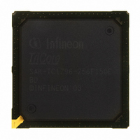
SAK-TC1796-256F150E BD Infineon Technologies, SAK-TC1796-256F150E BD Datasheet - Page 51

SAK-TC1796-256F150E BD
Manufacturer Part Number
SAK-TC1796-256F150E BD
Description
IC MCU 32BIT FLASH PG-BGA-416
Manufacturer
Infineon Technologies
Series
TC17xxr
Datasheet
1.SAK-TC1796-256F150E_BE.pdf
(134 pages)
Specifications of SAK-TC1796-256F150E BD
Core Processor
TriCore
Core Size
32-Bit
Speed
150MHz
Connectivity
ASC, CAN, EBI/EMI, MLI, MSC, SSC
Peripherals
DMA, POR, WDT
Number Of I /o
123
Program Memory Size
2MB (2M x 8)
Program Memory Type
FLASH
Ram Size
256K x 8
Voltage - Supply (vcc/vdd)
1.42 V ~ 1.58 V
Data Converters
A/D 44x12b
Oscillator Type
External
Operating Temperature
-40°C ~ 125°C
Package / Case
416-BGA
Packages
PG-BGA-416
Max Clock Frequency
150.0 MHz
Sram (incl. Cache)
256.0 KByte
Can Nodes
4
A / D Input Lines (incl. Fadc)
44
Program Memory
2.0 MB
For Use With
B158-H8537-G2-X-7600IN - KIT STARTER TC179X FAMILY
Lead Free Status / RoHS Status
Lead free / RoHS Compliant
Eeprom Size
-
Other names
KT1796256F150EBDXP
SAK-TC1796-256F150EBDIN
SP000228336
SAK-TC1796-256F150EBDIN
SP000228336
- Current page: 51 of 134
- Download datasheet (5Mb)
or can be received from an external master (Slave Mode). Data width, shift direction,
clock polarity and phase are programmable. This allows communication with SPI-
compatible devices. Transmission and reception of data is double-buffered. A shift clock
generator provides the SSC with a separate serial clock signal. One slave select input is
available for Slave Mode operation. Eight programmable slave select outputs (chip
selects) are supported in Master Mode. The I/O lines of the SSC0 module are connected
to dedicated device pins while the SSC1 module I/O lines are wired with general purpose
I/O port lines.
Features
•
•
•
•
•
•
•
•
Data Sheet
Master and Slave Mode operation
– Full-duplex or half-duplex operation
– Automatic pad control possible
Flexible data format
– Programmable number of data bits: 2 to 16 bits
– Programmable shift direction: LSB or MSB shift first
– Programmable clock polarity: Idle low or high state for the shift clock
– Programmable clock/data phase: data shift with leading or trailing edge of the shift
Baud rate generation from 37.5 Mbit/s to 572.2 Bit/s (@ 75 MHz module clock)
Interrupt generation
– On a transmitter empty condition
– On a receiver full condition
– On an error condition (receive, phase, baud rate, transmit error)
Flexible SSC pin configuration
One slave select input SLSI in slave mode
Eight programmable slave select outputs SLSO in Master Mode
– Automatic SLSO generation with programmable timing
– Programmable active level and enable control
SSC0 with 8-stage receive FIFO (RXFIFO) and 8-stage transmit FIFO (TXFIFO)
– Independent control of RXFIFO and TXFIFO
– 2- to 16-bit FIFO data width
– Programmable receive/transmit interrupt trigger level
– Receive and Transmit FIFO filling level indication
– Overrun error generation
– Underflow error generation
clock
51
Functional Description
V1.0, 2008-04
TC1796
Related parts for SAK-TC1796-256F150E BD
Image
Part Number
Description
Manufacturer
Datasheet
Request
R

Part Number:
Description:
IC MCU 32BIT FLASH 416-BGA
Manufacturer:
Infineon Technologies
Datasheet:

Part Number:
Description:
IC MCU 32BIT FLASH BGA-416
Manufacturer:
Infineon Technologies
Datasheet:

Part Number:
Description:
Manufacturer:
Infineon Technologies AG
Datasheet:

Part Number:
Description:
BGA 416/32 BIT FLASH
Manufacturer:
Infineon Technologies AG
Datasheet:

Part Number:
Description:
Manufacturer:
Infineon Technologies AG
Datasheet:

Part Number:
Description:
Manufacturer:
Infineon Technologies AG
Datasheet:

Part Number:
Description:
Manufacturer:
Infineon Technologies AG
Datasheet:

Part Number:
Description:
Manufacturer:
Infineon Technologies AG
Datasheet:

Part Number:
Description:
Manufacturer:
Infineon Technologies AG
Datasheet:

Part Number:
Description:
Manufacturer:
Infineon Technologies AG
Datasheet:

Part Number:
Description:
Manufacturer:
Infineon Technologies AG
Datasheet:

Part Number:
Description:
16-bit microcontroller with 2x2 KByte RAM
Manufacturer:
Infineon Technologies AG
Datasheet:

Part Number:
Description:
NPN silicon RF transistor
Manufacturer:
Infineon Technologies AG
Datasheet:

Part Number:
Description:
NPN silicon RF transistor
Manufacturer:
Infineon Technologies AG
Datasheet:

Part Number:
Description:
NPN silicon RF transistor
Manufacturer:
Infineon Technologies AG
Datasheet:


