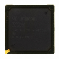
SAK-TC1796-256F150E BD Infineon Technologies, SAK-TC1796-256F150E BD Datasheet - Page 115

SAK-TC1796-256F150E BD
Manufacturer Part Number
SAK-TC1796-256F150E BD
Description
IC MCU 32BIT FLASH PG-BGA-416
Manufacturer
Infineon Technologies
Series
TC17xxr
Datasheet
1.SAK-TC1796-256F150E_BE.pdf
(134 pages)
Specifications of SAK-TC1796-256F150E BD
Core Processor
TriCore
Core Size
32-Bit
Speed
150MHz
Connectivity
ASC, CAN, EBI/EMI, MLI, MSC, SSC
Peripherals
DMA, POR, WDT
Number Of I /o
123
Program Memory Size
2MB (2M x 8)
Program Memory Type
FLASH
Ram Size
256K x 8
Voltage - Supply (vcc/vdd)
1.42 V ~ 1.58 V
Data Converters
A/D 44x12b
Oscillator Type
External
Operating Temperature
-40°C ~ 125°C
Package / Case
416-BGA
Packages
PG-BGA-416
Max Clock Frequency
150.0 MHz
Sram (incl. Cache)
256.0 KByte
Can Nodes
4
A / D Input Lines (incl. Fadc)
44
Program Memory
2.0 MB
For Use With
B158-H8537-G2-X-7600IN - KIT STARTER TC179X FAMILY
Lead Free Status / RoHS Status
Lead free / RoHS Compliant
Eeprom Size
-
Other names
KT1796256F150EBDXP
SAK-TC1796-256F150EBDIN
SP000228336
SAK-TC1796-256F150EBDIN
SP000228336
- Current page: 115 of 134
- Download datasheet (5Mb)
4.3.6
V
T
Table 25
Parameter
BFCLKO clock period
BFCLKO high time
BFCLKO low time
BFCLKO rise time
BFCLKO fall time
BFCLKO duty cycle
BFCLKO duty cycle
BFCLKO high time reduction
1) Not subject to production test, verified by design/characterization.
2) The PLL jitter characteristics add to this value according to the application settings. See the PLL jitter
3) The PLL jitter is not included in this parameter. If the BFCLKO frequency is equal to
4) The division ratio between LMB and BFCLKO frequency is set by EBU_BFCON.EXTCLOCK.
5) Due to asymmetry of the delays and slopes of the rising and falling edge of the pad. The influence of the PLL
Figure 34
Data Sheet
A
SS
parameters.
determines the duty cycle.
jitter is included in this parameter. This parameter should be applied taking the typical value of the duty cycle
in the account, not the minimum or maximum value.
= -40 °C to +125 °C;
= 0 V;
V
BFCLKO
BFCLKO Output Clock Timing
DD
BFCLK0 Output Clock Timing Parameters
BFCLKO Output Clock Timing
= 1.5 V ± 5%;
t
t
0.5
5
5
/(
/(
t
t
V
5
5
C
DDP05
+
+
L
t
t
= 35 pF
6
6
)
)
V
5)
3)
3)
DDEBU
Symbol
t
t
t
t
t
DC24
DC3
dt
BFCLKO
5
6
7
8
5
t
= 2.5 V ± 5% and 3.3 V ± 5%;
5
t
BFCLKO
CC 3
CC 3
CC –
CC –
CC 45
CC 30
CC –
CC 13.33
115
t
6
Min.
2)
t
Values
8
Typ.
–
–
–
–
–
50
33.33 36
–
1)
Max.
–
–
–
3
3
55
1.1
Electrical Parameters
t
7
MCT04883_mod
f
CPU
Unit Note /
ns
ns
ns
ns
ns
%
%
ns
0.9
0.1
, the K-divider setting
V
V
DD
DD
V1.0, 2008-04
Test Con
dition
–
–
–
–
–
divider of
2, 4, ...
divider of
3
C
L
4)
TC1796
= 20pF
4)
Related parts for SAK-TC1796-256F150E BD
Image
Part Number
Description
Manufacturer
Datasheet
Request
R

Part Number:
Description:
IC MCU 32BIT FLASH 416-BGA
Manufacturer:
Infineon Technologies
Datasheet:

Part Number:
Description:
IC MCU 32BIT FLASH BGA-416
Manufacturer:
Infineon Technologies
Datasheet:

Part Number:
Description:
Manufacturer:
Infineon Technologies AG
Datasheet:

Part Number:
Description:
BGA 416/32 BIT FLASH
Manufacturer:
Infineon Technologies AG
Datasheet:

Part Number:
Description:
Manufacturer:
Infineon Technologies AG
Datasheet:

Part Number:
Description:
Manufacturer:
Infineon Technologies AG
Datasheet:

Part Number:
Description:
Manufacturer:
Infineon Technologies AG
Datasheet:

Part Number:
Description:
Manufacturer:
Infineon Technologies AG
Datasheet:

Part Number:
Description:
Manufacturer:
Infineon Technologies AG
Datasheet:

Part Number:
Description:
Manufacturer:
Infineon Technologies AG
Datasheet:

Part Number:
Description:
Manufacturer:
Infineon Technologies AG
Datasheet:

Part Number:
Description:
16-bit microcontroller with 2x2 KByte RAM
Manufacturer:
Infineon Technologies AG
Datasheet:

Part Number:
Description:
NPN silicon RF transistor
Manufacturer:
Infineon Technologies AG
Datasheet:

Part Number:
Description:
NPN silicon RF transistor
Manufacturer:
Infineon Technologies AG
Datasheet:

Part Number:
Description:
NPN silicon RF transistor
Manufacturer:
Infineon Technologies AG
Datasheet:


