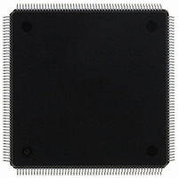
MCF5307AI90B Freescale Semiconductor, MCF5307AI90B Datasheet - Page 393

MCF5307AI90B
Manufacturer Part Number
MCF5307AI90B
Description
IC MPU 32BIT COLDF 90MHZ 208FQFP
Manufacturer
Freescale Semiconductor
Series
MCF530xr
Datasheets
1.MCF5307AI66B.pdf
(484 pages)
2.MCF5307AI66B.pdf
(16 pages)
3.MCF5307AI66B.pdf
(2 pages)
Specifications of MCF5307AI90B
Core Processor
Coldfire V3
Core Size
32-Bit
Speed
90MHz
Connectivity
EBI/EMI, I²C, UART/USART
Peripherals
DMA, POR, WDT
Number Of I /o
16
Program Memory Type
ROMless
Ram Size
4K x 8
Voltage - Supply (vcc/vdd)
3 V ~ 3.6 V
Oscillator Type
External
Operating Temperature
0°C ~ 70°C
Package / Case
208-FQFP
Maximum Clock Frequency
90 MHz
Maximum Operating Temperature
+ 105 C
Mounting Style
SMD/SMT
Minimum Operating Temperature
0 C
Family Name
MCF5xxx
Device Core
ColdFire
Device Core Size
32b
Frequency (max)
90MHz
Instruction Set Architecture
RISC
Supply Voltage 1 (typ)
3.3V
Operating Temp Range
0C to 70C
Operating Temperature Classification
Commercial
Mounting
Surface Mount
Pin Count
208
Package Type
FQFP
Program Memory Size
8KB
Cpu Speed
90MHz
Embedded Interface Type
I2C, UART
Digital Ic Case Style
FQFP
No. Of Pins
208
Supply Voltage Range
3V To 3.6V
Rohs Compliant
Yes
Lead Free Status / RoHS Status
Lead free / RoHS Compliant
Eeprom Size
-
Program Memory Size
-
Data Converters
-
Lead Free Status / Rohs Status
Lead free / RoHS Compliant
Available stocks
Company
Part Number
Manufacturer
Quantity
Price
Company:
Part Number:
MCF5307AI90B
Manufacturer:
FREESCAL
Quantity:
153
Company:
Part Number:
MCF5307AI90B
Manufacturer:
Freescale Semiconductor
Quantity:
10 000
Part Number:
MCF5307AI90B
Manufacturer:
FREESCALE
Quantity:
20 000
- Current page: 393 of 484
- Download datasheet (6Mb)
Table 18-3 shows the type of access as a function of match in the CSCRs and DACRs.
Basic bus operations occur in three clocks, as follows:
18.4.2 Data Transfer Cycle States
The data transfer operation in the MCF5307 is controlled by an on-chip state machine. Each
bus clock cycle is divided into two states. Even states occur when BCLKO is high and odd
states occur when BCLKO is low. The state transition diagram for basic and
fast-termination read and write cycles is shown in Figure 18-4.
1. During the first clock, the address, attributes, and TS are driven. AS is asserted at the
2. Data and TA are sampled during the second clock of a bus-read cycle. During a read,
3. The last clock of the bus cycle uses what would be an idle clock between cycles to
0
1
Multiple
0
1
Multiple
0
1
Multiple
falling edge of the clock to indicate that address and attributes are valid and stable.
the external device provides data and is sampled at the rising edge at the end of the
second bus clock. This data is concurrent with TA, which is also sampled at the
rising clock edge.
During a write, the MCF5307 drives data from the rising clock edge at the end of the
first clock to the rising clock edge at the end of the bus cycle. Wait states can be
added between the first and second clocks by delaying the assertion of TA. TA can
be configured to be generated internally through the DACRs and CSCRs. If TA is
not generated internally, the system must provide it externally.
provide hold time for address, attributes, and write data. Figure 18-6 and
Figure 18-8 show the basic read and write operations.
Number of CSCR Matches
Table 18-3. Accesses by Matches in CSCRs and DACRs
Freescale Semiconductor, Inc.
For More Information On This Product,
0
0
0
1
1
1
Multiple
Multiple
Multiple
Number of DACR Matches
Chapter 18. Bus Operation
Go to: www.freescale.com
External
Defined by CSCRs
External, burst-inhibited, 32-bit
Defined by DACRs
Undefined
Undefined
Undefined
Undefined
Undefined
Type of Access
Data Transfer Operation
18-5
Related parts for MCF5307AI90B
Image
Part Number
Description
Manufacturer
Datasheet
Request
R
Part Number:
Description:
Manufacturer:
Freescale Semiconductor, Inc
Datasheet:
Part Number:
Description:
Mcf5307 Coldfire Integrated Microprocessor User
Manufacturer:
Freescale Semiconductor, Inc
Datasheet:
Part Number:
Description:
Manufacturer:
Freescale Semiconductor, Inc
Datasheet:
Part Number:
Description:
Manufacturer:
Freescale Semiconductor, Inc
Datasheet:
Part Number:
Description:
Manufacturer:
Freescale Semiconductor, Inc
Datasheet:
Part Number:
Description:
Manufacturer:
Freescale Semiconductor, Inc
Datasheet:
Part Number:
Description:
Manufacturer:
Freescale Semiconductor, Inc
Datasheet:
Part Number:
Description:
Manufacturer:
Freescale Semiconductor, Inc
Datasheet:
Part Number:
Description:
Manufacturer:
Freescale Semiconductor, Inc
Datasheet:
Part Number:
Description:
Manufacturer:
Freescale Semiconductor, Inc
Datasheet:
Part Number:
Description:
Manufacturer:
Freescale Semiconductor, Inc
Datasheet:
Part Number:
Description:
Manufacturer:
Freescale Semiconductor, Inc
Datasheet:
Part Number:
Description:
Manufacturer:
Freescale Semiconductor, Inc
Datasheet:
Part Number:
Description:
Manufacturer:
Freescale Semiconductor, Inc
Datasheet:
Part Number:
Description:
Manufacturer:
Freescale Semiconductor, Inc
Datasheet:


