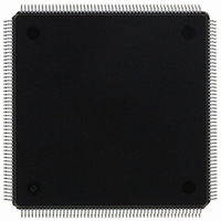
MCF5307AI90B Freescale Semiconductor, MCF5307AI90B Datasheet - Page 256

MCF5307AI90B
Manufacturer Part Number
MCF5307AI90B
Description
IC MPU 32BIT COLDF 90MHZ 208FQFP
Manufacturer
Freescale Semiconductor
Series
MCF530xr
Datasheets
1.MCF5307AI66B.pdf
(484 pages)
2.MCF5307AI66B.pdf
(16 pages)
3.MCF5307AI66B.pdf
(2 pages)
Specifications of MCF5307AI90B
Core Processor
Coldfire V3
Core Size
32-Bit
Speed
90MHz
Connectivity
EBI/EMI, I²C, UART/USART
Peripherals
DMA, POR, WDT
Number Of I /o
16
Program Memory Type
ROMless
Ram Size
4K x 8
Voltage - Supply (vcc/vdd)
3 V ~ 3.6 V
Oscillator Type
External
Operating Temperature
0°C ~ 70°C
Package / Case
208-FQFP
Maximum Clock Frequency
90 MHz
Maximum Operating Temperature
+ 105 C
Mounting Style
SMD/SMT
Minimum Operating Temperature
0 C
Family Name
MCF5xxx
Device Core
ColdFire
Device Core Size
32b
Frequency (max)
90MHz
Instruction Set Architecture
RISC
Supply Voltage 1 (typ)
3.3V
Operating Temp Range
0C to 70C
Operating Temperature Classification
Commercial
Mounting
Surface Mount
Pin Count
208
Package Type
FQFP
Program Memory Size
8KB
Cpu Speed
90MHz
Embedded Interface Type
I2C, UART
Digital Ic Case Style
FQFP
No. Of Pins
208
Supply Voltage Range
3V To 3.6V
Rohs Compliant
Yes
Lead Free Status / RoHS Status
Lead free / RoHS Compliant
Eeprom Size
-
Program Memory Size
-
Data Converters
-
Lead Free Status / Rohs Status
Lead free / RoHS Compliant
Available stocks
Company
Part Number
Manufacturer
Quantity
Price
Company:
Part Number:
MCF5307AI90B
Manufacturer:
FREESCAL
Quantity:
153
Company:
Part Number:
MCF5307AI90B
Manufacturer:
Freescale Semiconductor
Quantity:
10 000
Part Number:
MCF5307AI90B
Manufacturer:
FREESCALE
Quantity:
20 000
- Current page: 256 of 484
- Download datasheet (6Mb)
Synchronous Operation
11.4.3.3 DRAM Controller Mask Registers (DMR0/DMR1)
The DMRn, Figure 11-17, include mask bits for the base address and for address attributes.
They are the same as in asynchronous operation.
Table 11-14 describes DMRn fields.
6
5–4
3
2
1–0
11-22
Reset
Table 11-13. DACR0/DACR1 Field Descriptions (Synchronous Mode) (Continued)
Field
Addr
Bit
R/W
31
Name
IMRS Initiate mode register set (
PM
PS
—
IP
Figure 11-17. DRAM Controller Mask Registers (DMR0 and DMR1)
associated SDRAMs. In initialization, IMRS should be set only after all DRAM controller registers are
initialized and
an SDRAM block programs the SDRAM’s mode register. Thus, the address of the access should be
programmed to place the correct mode information on the SDRAM address pins. Because the
SDRAM does not register this information, it doesn’t matter if the IMRS access is a read or a write or
what, if any, data is put onto the data bus. The DRAM controller clears IMRS after the
finishes.
0 Take no action
1 Initiate
Port size. Indicates the port size of the associated block of SDRAM, which allows for dynamic sizing
of associated SDRAM accesses. PS functions the same in asynchronous operation.
00 32-bit port
01 8-bit port
1x 16-bit port
Initiate precharge all (
finished. Accesses via IP should be no wider than the port size programmed in PS.
0 Take no action.
1 A
Page mode. Indicates how the associated SDRAM block supports page-mode operation.
0 Page mode on bursts only. The DRAM controller dynamically bursts the transfer if it falls within a
1 Continuous page mode. The page stays open and only SCAS needs to be asserted for sequential
Reserved, should be cleared.
executed after all DRAM controller registers are programmed. After IP is set, the next write to an
appropriate SDRAM address generates the
single page and the transfer size exceeds the port size of the SDRAM block. After the burst, the
page closes and a precharge is issued.
SDRAM accesses that hit in the same page, regardless of whether the access is a burst.
PALL
BAM
command is sent to the associated SDRAM block. During initialization, this command is
MRS
Freescale Semiconductor, Inc.
command
PALL
For More Information On This Product,
and
PALL
REFRESH
MBAR + 0x10C (DMR0), 0x114 (DMR1)
MRS
) command. The DRAM controller clears IP after the
Go to: www.freescale.com
MCF5307 User’s Manual
18 17
) command. Setting IMRS generates a
commands have been issued. After IMRS is set, the next access to
Uninitialized
R/W
Description
—
PALL
command to the SDRAM block.
9
WP — C/I AM SC SD UC UD V
8
7
MRS
6
command to the
5
PALL
4
command is
MRS
3
command
2
1
0
0
Related parts for MCF5307AI90B
Image
Part Number
Description
Manufacturer
Datasheet
Request
R
Part Number:
Description:
Manufacturer:
Freescale Semiconductor, Inc
Datasheet:
Part Number:
Description:
Mcf5307 Coldfire Integrated Microprocessor User
Manufacturer:
Freescale Semiconductor, Inc
Datasheet:
Part Number:
Description:
Manufacturer:
Freescale Semiconductor, Inc
Datasheet:
Part Number:
Description:
Manufacturer:
Freescale Semiconductor, Inc
Datasheet:
Part Number:
Description:
Manufacturer:
Freescale Semiconductor, Inc
Datasheet:
Part Number:
Description:
Manufacturer:
Freescale Semiconductor, Inc
Datasheet:
Part Number:
Description:
Manufacturer:
Freescale Semiconductor, Inc
Datasheet:
Part Number:
Description:
Manufacturer:
Freescale Semiconductor, Inc
Datasheet:
Part Number:
Description:
Manufacturer:
Freescale Semiconductor, Inc
Datasheet:
Part Number:
Description:
Manufacturer:
Freescale Semiconductor, Inc
Datasheet:
Part Number:
Description:
Manufacturer:
Freescale Semiconductor, Inc
Datasheet:
Part Number:
Description:
Manufacturer:
Freescale Semiconductor, Inc
Datasheet:
Part Number:
Description:
Manufacturer:
Freescale Semiconductor, Inc
Datasheet:
Part Number:
Description:
Manufacturer:
Freescale Semiconductor, Inc
Datasheet:
Part Number:
Description:
Manufacturer:
Freescale Semiconductor, Inc
Datasheet:


