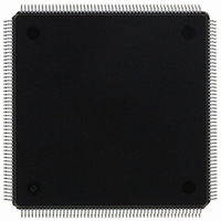
MCF5307AI90B Freescale Semiconductor, MCF5307AI90B Datasheet - Page 140

MCF5307AI90B
Manufacturer Part Number
MCF5307AI90B
Description
IC MPU 32BIT COLDF 90MHZ 208FQFP
Manufacturer
Freescale Semiconductor
Series
MCF530xr
Datasheets
1.MCF5307AI66B.pdf
(484 pages)
2.MCF5307AI66B.pdf
(16 pages)
3.MCF5307AI66B.pdf
(2 pages)
Specifications of MCF5307AI90B
Core Processor
Coldfire V3
Core Size
32-Bit
Speed
90MHz
Connectivity
EBI/EMI, I²C, UART/USART
Peripherals
DMA, POR, WDT
Number Of I /o
16
Program Memory Type
ROMless
Ram Size
4K x 8
Voltage - Supply (vcc/vdd)
3 V ~ 3.6 V
Oscillator Type
External
Operating Temperature
0°C ~ 70°C
Package / Case
208-FQFP
Maximum Clock Frequency
90 MHz
Maximum Operating Temperature
+ 105 C
Mounting Style
SMD/SMT
Minimum Operating Temperature
0 C
Family Name
MCF5xxx
Device Core
ColdFire
Device Core Size
32b
Frequency (max)
90MHz
Instruction Set Architecture
RISC
Supply Voltage 1 (typ)
3.3V
Operating Temp Range
0C to 70C
Operating Temperature Classification
Commercial
Mounting
Surface Mount
Pin Count
208
Package Type
FQFP
Program Memory Size
8KB
Cpu Speed
90MHz
Embedded Interface Type
I2C, UART
Digital Ic Case Style
FQFP
No. Of Pins
208
Supply Voltage Range
3V To 3.6V
Rohs Compliant
Yes
Lead Free Status / RoHS Status
Lead free / RoHS Compliant
Eeprom Size
-
Program Memory Size
-
Data Converters
-
Lead Free Status / Rohs Status
Lead free / RoHS Compliant
Available stocks
Company
Part Number
Manufacturer
Quantity
Price
Company:
Part Number:
MCF5307AI90B
Manufacturer:
FREESCAL
Quantity:
153
Company:
Part Number:
MCF5307AI90B
Manufacturer:
Freescale Semiconductor
Quantity:
10 000
Part Number:
MCF5307AI90B
Manufacturer:
FREESCALE
Quantity:
20 000
- Current page: 140 of 484
- Download datasheet (6Mb)
Programming Model
5.4.5 Data Breakpoint/Mask Registers (DBR, DBMR)
The data breakpoint registers, Figure 5-9, specify data patterns used as part of the trigger
into debug mode. Only DBR bits not masked with a corresponding zero in DBMR are
compared with the data from the processor’s local bus, as defined in TDR.
DRc[4–0]
5-12
9–8
3–0
Bit
10
7
6
5
4
Reset
Field
R/W DBR is accessible in supervisor mode as debug control register 0x0E, using the WDEBUG instruction and
UHE
BTB
NPL
SSM
Name
through the BDM port using the
DBMR is accessible in supervisor mode as debug control register 0x0F using the WDEBUG instruction and
via the BDM port using the
IPI
—
—
31
Figure 5-9. Data Breakpoint/Mask Registers (DBR and DBMR)
User halt enable. Selects the CPU privilege level required to execute the HALT instruction.
0 HALT is a supervisor-only instruction.
1 HALT is a supervisor/user instruction.
Branch target bytes. Defines the number of bytes of branch target address DDATA displays.
00 0 bytes
01 Lower 2 bytes of the target address
10 Lower 3 bytes of the target address
11 Entire 4-byte target address
See Section 5.3.1, “Begin Execution of Taken Branch (PST = 0x5).”
Reserved, should be cleared.
Non-pipelined mode. Determines whether the core operates in pipelined or mode or not.
0 Pipelined mode
1 Nonpipelined mode. The processor effectively executes one instruction at a time with no overlap.
Regardless of the NPL state, a triggered PC breakpoint is always reported before the triggering
instruction executes. In normal pipeline operation, the occurrence of an address and/or data
breakpoint trigger is imprecise. In non-pipeline mode, triggers are always reported before the next
instruction begins execution and trigger reporting can be considered precise.
An address or data breakpoint should always occur before the next instruction begins execution.
Therefore the occurrence of the address/data breakpoints should be guaranteed.
Ignore pending interrupts.
1 Core ignores any pending interrupt requests signalled while in single-instruction-step mode.
0 Core services any pending interrupt requests that were signalled while in single-step mode.
Single-step mode. Setting SSM puts the processor in single-step mode.
0 Normal mode.
1 Single-step mode. The processor halts after execution of each instruction. While halted, any
Reserved, should be cleared.
This adds at least 5 cycles to the execution time of each instruction. Instruction folding is
disabled. Given an average execution latency of 1.6, throughput in non-pipeline mode would be
6.6, approximately 25% or less of pipelined performance.
BDM command can be executed. On receipt of the
next instruction and halts again. This process continues until SSM is cleared.
Table 5-8. CSR Field Descriptions (Continued)
Freescale Semiconductor, Inc.
For More Information On This Product,
WDMREG
RDMREG
Go to: www.freescale.com
MCF5307 User’s Manual
command.
0x0E (DBR), 0x0F (DBMR)
Data (DBR); Mask (DBMR)
and
WDMREG
Uninitialized
Description
commands.
GO
command, the processor executes the
0
Related parts for MCF5307AI90B
Image
Part Number
Description
Manufacturer
Datasheet
Request
R
Part Number:
Description:
Manufacturer:
Freescale Semiconductor, Inc
Datasheet:
Part Number:
Description:
Mcf5307 Coldfire Integrated Microprocessor User
Manufacturer:
Freescale Semiconductor, Inc
Datasheet:
Part Number:
Description:
Manufacturer:
Freescale Semiconductor, Inc
Datasheet:
Part Number:
Description:
Manufacturer:
Freescale Semiconductor, Inc
Datasheet:
Part Number:
Description:
Manufacturer:
Freescale Semiconductor, Inc
Datasheet:
Part Number:
Description:
Manufacturer:
Freescale Semiconductor, Inc
Datasheet:
Part Number:
Description:
Manufacturer:
Freescale Semiconductor, Inc
Datasheet:
Part Number:
Description:
Manufacturer:
Freescale Semiconductor, Inc
Datasheet:
Part Number:
Description:
Manufacturer:
Freescale Semiconductor, Inc
Datasheet:
Part Number:
Description:
Manufacturer:
Freescale Semiconductor, Inc
Datasheet:
Part Number:
Description:
Manufacturer:
Freescale Semiconductor, Inc
Datasheet:
Part Number:
Description:
Manufacturer:
Freescale Semiconductor, Inc
Datasheet:
Part Number:
Description:
Manufacturer:
Freescale Semiconductor, Inc
Datasheet:
Part Number:
Description:
Manufacturer:
Freescale Semiconductor, Inc
Datasheet:
Part Number:
Description:
Manufacturer:
Freescale Semiconductor, Inc
Datasheet:


