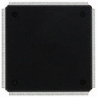
MCF5307AI90B Freescale Semiconductor, MCF5307AI90B Datasheet - Page 240

MCF5307AI90B
Manufacturer Part Number
MCF5307AI90B
Description
IC MPU 32BIT COLDF 90MHZ 208FQFP
Manufacturer
Freescale Semiconductor
Series
MCF530xr
Datasheets
1.MCF5307AI66B.pdf
(484 pages)
2.MCF5307AI66B.pdf
(16 pages)
3.MCF5307AI66B.pdf
(2 pages)
Specifications of MCF5307AI90B
Core Processor
Coldfire V3
Core Size
32-Bit
Speed
90MHz
Connectivity
EBI/EMI, I²C, UART/USART
Peripherals
DMA, POR, WDT
Number Of I /o
16
Program Memory Type
ROMless
Ram Size
4K x 8
Voltage - Supply (vcc/vdd)
3 V ~ 3.6 V
Oscillator Type
External
Operating Temperature
0°C ~ 70°C
Package / Case
208-FQFP
Maximum Clock Frequency
90 MHz
Maximum Operating Temperature
+ 105 C
Mounting Style
SMD/SMT
Minimum Operating Temperature
0 C
Family Name
MCF5xxx
Device Core
ColdFire
Device Core Size
32b
Frequency (max)
90MHz
Instruction Set Architecture
RISC
Supply Voltage 1 (typ)
3.3V
Operating Temp Range
0C to 70C
Operating Temperature Classification
Commercial
Mounting
Surface Mount
Pin Count
208
Package Type
FQFP
Program Memory Size
8KB
Cpu Speed
90MHz
Embedded Interface Type
I2C, UART
Digital Ic Case Style
FQFP
No. Of Pins
208
Supply Voltage Range
3V To 3.6V
Rohs Compliant
Yes
Lead Free Status / RoHS Status
Lead free / RoHS Compliant
Eeprom Size
-
Program Memory Size
-
Data Converters
-
Lead Free Status / Rohs Status
Lead free / RoHS Compliant
Available stocks
Company
Part Number
Manufacturer
Quantity
Price
Company:
Part Number:
MCF5307AI90B
Manufacturer:
FREESCAL
Quantity:
153
Company:
Part Number:
MCF5307AI90B
Manufacturer:
Freescale Semiconductor
Quantity:
10 000
Part Number:
MCF5307AI90B
Manufacturer:
FREESCALE
Quantity:
20 000
- Current page: 240 of 484
- Download datasheet (6Mb)
Asynchronous Operation
Table 11-4 describes DACRn fields.
11-6
Reset
31–18
17–16
13–12
11–10
Field
Addr
Bits
R/W
15
14
9
8
7
6
31
RNCN RAS-negate-to-CAS-negate. Controls whether RAS and CAS negate concurrently or one clock
Name
RCD
EDO
Figure 11-3. DRAM Address and Control Registers (DACR0/DACR1)
CAS
BA
RE
RP
—
—
—
Base address. Used with DMR[BAM] to determine the address range in which the associated
DRAM block is located. Each BA bit is compared with the corresponding address of the bus cycle in
progress. If each bit matches, or if bits that do not match are masked in the BAM, the address
selects the associated DRAM block.
Reserved, should be cleared.
Refresh enable. Determines whether the DRAM controller generates a refresh to the associated
DRAM block. DRAM contents are not preserved during hard reset or software watchdog reset.
0 Do not refresh associated DRAM block. (Default at reset)
1 Refresh associated DRAM block.
Reserved, should be cleared.
CAS timing. Determines how long CAS is asserted during a DRAM access.
00 1 clock cycle
01 2 clock cycles
10 3 clock cycles
11 4 clock cycles
RAS precharge timing. Determines how long RAS is precharged between accesses. Note that RP
is different from DCR[RRP].
00 1 clock cycle
01 2 clock cycles
10 3 clock cycles
11 4 clock cycles
apart. RNCN is ignored if CAS is asserted for only one clock and both RAS and CAS are negated.
RNCN is used only for non-page-mode accesses and single accesses in page mode.
0 RAS negates concurrently with CAS.
1 RAS negates one clock before CAS.
RAS-to-CAS delay. Determines the number of system clocks between assertions of RAS and CAS.
0 1 clock cycle
1 2 clock cycles
Reserved, should be cleared.
Extended data out. Determines whether the DRAM block operates in a mode to take advantage of
industry-standard EDO DRAMs. Do not use EDO mode with non-EDO DRAM.
0 EDO operation disabled.
1 EDO operation enabled.
Unitialized
BA
Table 11-4. DACR0/DACR1 Field Description
Freescale Semiconductor, Inc.
For More Information On This Product,
18 17 16
MBAR + 0x10C (DACR0); 0x110 (DACR1)
Go to: www.freescale.com
—
MCF5307 User’s Manual
RE — CAS
15
0
14 13 12 11 10
R/W
Description
RP
RNCN RCD — EDO
9
Unitialized
8
7
6
5
PS
4
3
PM
2
1
—
0
Related parts for MCF5307AI90B
Image
Part Number
Description
Manufacturer
Datasheet
Request
R
Part Number:
Description:
Manufacturer:
Freescale Semiconductor, Inc
Datasheet:
Part Number:
Description:
Mcf5307 Coldfire Integrated Microprocessor User
Manufacturer:
Freescale Semiconductor, Inc
Datasheet:
Part Number:
Description:
Manufacturer:
Freescale Semiconductor, Inc
Datasheet:
Part Number:
Description:
Manufacturer:
Freescale Semiconductor, Inc
Datasheet:
Part Number:
Description:
Manufacturer:
Freescale Semiconductor, Inc
Datasheet:
Part Number:
Description:
Manufacturer:
Freescale Semiconductor, Inc
Datasheet:
Part Number:
Description:
Manufacturer:
Freescale Semiconductor, Inc
Datasheet:
Part Number:
Description:
Manufacturer:
Freescale Semiconductor, Inc
Datasheet:
Part Number:
Description:
Manufacturer:
Freescale Semiconductor, Inc
Datasheet:
Part Number:
Description:
Manufacturer:
Freescale Semiconductor, Inc
Datasheet:
Part Number:
Description:
Manufacturer:
Freescale Semiconductor, Inc
Datasheet:
Part Number:
Description:
Manufacturer:
Freescale Semiconductor, Inc
Datasheet:
Part Number:
Description:
Manufacturer:
Freescale Semiconductor, Inc
Datasheet:
Part Number:
Description:
Manufacturer:
Freescale Semiconductor, Inc
Datasheet:
Part Number:
Description:
Manufacturer:
Freescale Semiconductor, Inc
Datasheet:


