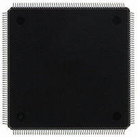
MCF5307AI90B Freescale Semiconductor, MCF5307AI90B Datasheet - Page 371

MCF5307AI90B
Manufacturer Part Number
MCF5307AI90B
Description
IC MPU 32BIT COLDF 90MHZ 208FQFP
Manufacturer
Freescale Semiconductor
Series
MCF530xr
Datasheets
1.MCF5307AI66B.pdf
(484 pages)
2.MCF5307AI66B.pdf
(16 pages)
3.MCF5307AI66B.pdf
(2 pages)
Specifications of MCF5307AI90B
Core Processor
Coldfire V3
Core Size
32-Bit
Speed
90MHz
Connectivity
EBI/EMI, I²C, UART/USART
Peripherals
DMA, POR, WDT
Number Of I /o
16
Program Memory Type
ROMless
Ram Size
4K x 8
Voltage - Supply (vcc/vdd)
3 V ~ 3.6 V
Oscillator Type
External
Operating Temperature
0°C ~ 70°C
Package / Case
208-FQFP
Maximum Clock Frequency
90 MHz
Maximum Operating Temperature
+ 105 C
Mounting Style
SMD/SMT
Minimum Operating Temperature
0 C
Family Name
MCF5xxx
Device Core
ColdFire
Device Core Size
32b
Frequency (max)
90MHz
Instruction Set Architecture
RISC
Supply Voltage 1 (typ)
3.3V
Operating Temp Range
0C to 70C
Operating Temperature Classification
Commercial
Mounting
Surface Mount
Pin Count
208
Package Type
FQFP
Program Memory Size
8KB
Cpu Speed
90MHz
Embedded Interface Type
I2C, UART
Digital Ic Case Style
FQFP
No. Of Pins
208
Supply Voltage Range
3V To 3.6V
Rohs Compliant
Yes
Lead Free Status / RoHS Status
Lead free / RoHS Compliant
Eeprom Size
-
Program Memory Size
-
Data Converters
-
Lead Free Status / Rohs Status
Lead free / RoHS Compliant
Available stocks
Company
Part Number
Manufacturer
Quantity
Price
Company:
Part Number:
MCF5307AI90B
Manufacturer:
FREESCAL
Quantity:
153
Company:
Part Number:
MCF5307AI90B
Manufacturer:
Freescale Semiconductor
Quantity:
10 000
Part Number:
MCF5307AI90B
Manufacturer:
FREESCALE
Quantity:
20 000
- Current page: 371 of 484
- Download datasheet (6Mb)
17.2 MCF5307 Bus Signals
The bus signals provide the external bus interface to the MCF5307.
17.2.1 Address Bus
The address bus provides the address of the byte or most-significant byte (MSB) of the
word or longword being transferred. The address lines also serve as the DRAM addressing,
providing multiplexed row and column address signals. When an external device has
ownership of the MCF5307 bus, the device must drive the address bus and assert TS or AS
to indicate the start of a bus cycle. During an interrupt acknowledge access, A[4:2] indicate
the interrupt level being acknowledged.
17.2.1.1 Address Bus (A[23:0])
The lower 24 bits of the address bus become valid when TS is asserted. A[4:2] indicate the
interrupt level during interrupt acknowledge cycles.
17.2.1.2 Address Bus (A[31:24]/PP[15:8])
These multiplexed pins can serve as the most-significant byte of the address bus, or as the
most-significant byte of the parallel port. Programming the PAR in the system integration
module (SIM) determines the function of each of these eight multiplexed pins. These pins
are programmable on a bit-by-bit basis.
SRAS
TA
TCK
TDI/DSI
TDO/DSO
TIN[1:0]
TIP
TMS/BKPT
TM[2:0]
TOUT[1:0]
TRST/DSCLK
TS
TT[1:0]
TxD[1:0]
Abbreviation
Table 17-2. MCF507 Alphabetical Signal Index (Continued)
Synchronous row address strobe
Transfer acknowledge
Test clock
Test data input/Development serial input
Test data output/Development serial output
Timer input
Transfer in progress
Test mode select/Breakpoint
Transfer modifier
Timer outputs
Test reset/Development serial clock
Transfer start
Transfer type
Transmit data
Freescale Semiconductor, Inc.
For More Information On This Product,
Chapter 17. Signal Descriptions
Signal Name
Go to: www.freescale.com
DRAM
Bus
JTAG
JTAG
JTAG
Timer
Bus
JTAG
Bus
Timer
JTAG
Bus
Bus
Serial module
Function
MCF5307 Bus Signals
I/O
I/O
I/O
O
O
O
O
O
O
O
I
I
I
I
I
17-17
17-23
17-22
17-22
17-19
17-10
17-22
17-10
17-19
17-21
17-10
17-18
Page
17-9
17-9
17-7
Related parts for MCF5307AI90B
Image
Part Number
Description
Manufacturer
Datasheet
Request
R
Part Number:
Description:
Manufacturer:
Freescale Semiconductor, Inc
Datasheet:
Part Number:
Description:
Mcf5307 Coldfire Integrated Microprocessor User
Manufacturer:
Freescale Semiconductor, Inc
Datasheet:
Part Number:
Description:
Manufacturer:
Freescale Semiconductor, Inc
Datasheet:
Part Number:
Description:
Manufacturer:
Freescale Semiconductor, Inc
Datasheet:
Part Number:
Description:
Manufacturer:
Freescale Semiconductor, Inc
Datasheet:
Part Number:
Description:
Manufacturer:
Freescale Semiconductor, Inc
Datasheet:
Part Number:
Description:
Manufacturer:
Freescale Semiconductor, Inc
Datasheet:
Part Number:
Description:
Manufacturer:
Freescale Semiconductor, Inc
Datasheet:
Part Number:
Description:
Manufacturer:
Freescale Semiconductor, Inc
Datasheet:
Part Number:
Description:
Manufacturer:
Freescale Semiconductor, Inc
Datasheet:
Part Number:
Description:
Manufacturer:
Freescale Semiconductor, Inc
Datasheet:
Part Number:
Description:
Manufacturer:
Freescale Semiconductor, Inc
Datasheet:
Part Number:
Description:
Manufacturer:
Freescale Semiconductor, Inc
Datasheet:
Part Number:
Description:
Manufacturer:
Freescale Semiconductor, Inc
Datasheet:
Part Number:
Description:
Manufacturer:
Freescale Semiconductor, Inc
Datasheet:


