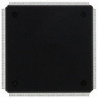
MCF5307AI90B Freescale Semiconductor, MCF5307AI90B Datasheet - Page 182

MCF5307AI90B
Manufacturer Part Number
MCF5307AI90B
Description
IC MPU 32BIT COLDF 90MHZ 208FQFP
Manufacturer
Freescale Semiconductor
Series
MCF530xr
Datasheets
1.MCF5307AI66B.pdf
(484 pages)
2.MCF5307AI66B.pdf
(16 pages)
3.MCF5307AI66B.pdf
(2 pages)
Specifications of MCF5307AI90B
Core Processor
Coldfire V3
Core Size
32-Bit
Speed
90MHz
Connectivity
EBI/EMI, I²C, UART/USART
Peripherals
DMA, POR, WDT
Number Of I /o
16
Program Memory Type
ROMless
Ram Size
4K x 8
Voltage - Supply (vcc/vdd)
3 V ~ 3.6 V
Oscillator Type
External
Operating Temperature
0°C ~ 70°C
Package / Case
208-FQFP
Maximum Clock Frequency
90 MHz
Maximum Operating Temperature
+ 105 C
Mounting Style
SMD/SMT
Minimum Operating Temperature
0 C
Family Name
MCF5xxx
Device Core
ColdFire
Device Core Size
32b
Frequency (max)
90MHz
Instruction Set Architecture
RISC
Supply Voltage 1 (typ)
3.3V
Operating Temp Range
0C to 70C
Operating Temperature Classification
Commercial
Mounting
Surface Mount
Pin Count
208
Package Type
FQFP
Program Memory Size
8KB
Cpu Speed
90MHz
Embedded Interface Type
I2C, UART
Digital Ic Case Style
FQFP
No. Of Pins
208
Supply Voltage Range
3V To 3.6V
Rohs Compliant
Yes
Lead Free Status / RoHS Status
Lead free / RoHS Compliant
Eeprom Size
-
Program Memory Size
-
Data Converters
-
Lead Free Status / Rohs Status
Lead free / RoHS Compliant
Available stocks
Company
Part Number
Manufacturer
Quantity
Price
Company:
Part Number:
MCF5307AI90B
Manufacturer:
FREESCAL
Quantity:
153
Company:
Part Number:
MCF5307AI90B
Manufacturer:
Freescale Semiconductor
Quantity:
10 000
Part Number:
MCF5307AI90B
Manufacturer:
FREESCALE
Quantity:
20 000
- Current page: 182 of 484
- Download datasheet (6Mb)
Features
The following is a list of the key SIM features:
6-2
• Module base address register (MBAR)
• Phase-locked loop (PLL) clock control register (PLLCR) for CPU STOP instruction
• Interrupt controller
• Chip select module
• System protection and reset status
• Pin assignment register (PAR) configures the parallel port. See Section 6.2.9, “Pin
• Bus arbitration
— Base address location of all internal peripherals and SIM resources
— Address space masking to internal peripherals and SIM resources
— Control for turning off clocks to core and interrupt levels that turn clocks back on
Chapter 7, “Phase-Locked Loop (PLL).”
— Programmable interrupt level (1–7) for internal peripheral interrupts
— Programmable priority level (0–3) within each interrupt level
— Four external interrupts; one set to interrupt level 7; three others programmable
See Chapter 9, “Interrupt Controller.”
— Eight independent, user-programmable chip-select signals (CS[7:0]) that can
— Address masking for 64-Kbyte to 4-Gbyte memory block sizes
— Programmable wait states and port sizes
— External master access to chip selects
See Chapter 10, “Chip-Select Module.”
— Reset status indicating the cause of last reset
— Software watchdog timer with programmable secondary bus monitor
See Section 6.2.4, “Software Watchdog Timer.”
Assignment Register (PAR).”
— Default bus master park register (MPARK) controls internal and external bus
— Supports several arbitration algorithms
See Section 6.2.10, “Bus Arbitration Control.”
to two interrupt levels
interface with SRAM, PROM, EPROM, EEPROM, Flash, and peripherals
arbitration and enables display of internal accesses on the external bus for
debugging
Freescale Semiconductor, Inc.
For More Information On This Product,
Go to: www.freescale.com
MCF5307 User’s Manual
Related parts for MCF5307AI90B
Image
Part Number
Description
Manufacturer
Datasheet
Request
R
Part Number:
Description:
Manufacturer:
Freescale Semiconductor, Inc
Datasheet:
Part Number:
Description:
Mcf5307 Coldfire Integrated Microprocessor User
Manufacturer:
Freescale Semiconductor, Inc
Datasheet:
Part Number:
Description:
Manufacturer:
Freescale Semiconductor, Inc
Datasheet:
Part Number:
Description:
Manufacturer:
Freescale Semiconductor, Inc
Datasheet:
Part Number:
Description:
Manufacturer:
Freescale Semiconductor, Inc
Datasheet:
Part Number:
Description:
Manufacturer:
Freescale Semiconductor, Inc
Datasheet:
Part Number:
Description:
Manufacturer:
Freescale Semiconductor, Inc
Datasheet:
Part Number:
Description:
Manufacturer:
Freescale Semiconductor, Inc
Datasheet:
Part Number:
Description:
Manufacturer:
Freescale Semiconductor, Inc
Datasheet:
Part Number:
Description:
Manufacturer:
Freescale Semiconductor, Inc
Datasheet:
Part Number:
Description:
Manufacturer:
Freescale Semiconductor, Inc
Datasheet:
Part Number:
Description:
Manufacturer:
Freescale Semiconductor, Inc
Datasheet:
Part Number:
Description:
Manufacturer:
Freescale Semiconductor, Inc
Datasheet:
Part Number:
Description:
Manufacturer:
Freescale Semiconductor, Inc
Datasheet:
Part Number:
Description:
Manufacturer:
Freescale Semiconductor, Inc
Datasheet:


