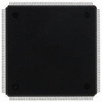
MCF5307AI90B Freescale Semiconductor, MCF5307AI90B Datasheet - Page 383

MCF5307AI90B
Manufacturer Part Number
MCF5307AI90B
Description
IC MPU 32BIT COLDF 90MHZ 208FQFP
Manufacturer
Freescale Semiconductor
Series
MCF530xr
Datasheets
1.MCF5307AI66B.pdf
(484 pages)
2.MCF5307AI66B.pdf
(16 pages)
3.MCF5307AI66B.pdf
(2 pages)
Specifications of MCF5307AI90B
Core Processor
Coldfire V3
Core Size
32-Bit
Speed
90MHz
Connectivity
EBI/EMI, I²C, UART/USART
Peripherals
DMA, POR, WDT
Number Of I /o
16
Program Memory Type
ROMless
Ram Size
4K x 8
Voltage - Supply (vcc/vdd)
3 V ~ 3.6 V
Oscillator Type
External
Operating Temperature
0°C ~ 70°C
Package / Case
208-FQFP
Maximum Clock Frequency
90 MHz
Maximum Operating Temperature
+ 105 C
Mounting Style
SMD/SMT
Minimum Operating Temperature
0 C
Family Name
MCF5xxx
Device Core
ColdFire
Device Core Size
32b
Frequency (max)
90MHz
Instruction Set Architecture
RISC
Supply Voltage 1 (typ)
3.3V
Operating Temp Range
0C to 70C
Operating Temperature Classification
Commercial
Mounting
Surface Mount
Pin Count
208
Package Type
FQFP
Program Memory Size
8KB
Cpu Speed
90MHz
Embedded Interface Type
I2C, UART
Digital Ic Case Style
FQFP
No. Of Pins
208
Supply Voltage Range
3V To 3.6V
Rohs Compliant
Yes
Lead Free Status / RoHS Status
Lead free / RoHS Compliant
Eeprom Size
-
Program Memory Size
-
Data Converters
-
Lead Free Status / Rohs Status
Lead free / RoHS Compliant
Available stocks
Company
Part Number
Manufacturer
Quantity
Price
Company:
Part Number:
MCF5307AI90B
Manufacturer:
FREESCAL
Quantity:
153
Company:
Part Number:
MCF5307AI90B
Manufacturer:
Freescale Semiconductor
Quantity:
10 000
Part Number:
MCF5307AI90B
Manufacturer:
FREESCALE
Quantity:
20 000
- Current page: 383 of 484
- Download datasheet (6Mb)
17.10.1 Timer Inputs (TIN[1:0])
TIN[1:0] can be programmed as clocks that cause events in the counter and prescalers.
They can also cause captures on the rising edge, falling edge, or both edges.
17.10.2 Timer Outputs (TOUT1, TOUT0)
The programmable timer outputs (TOUT1 and TOUT0) pulse or toggle on various timer
events.
17.11 Parallel I/O Port (PP[15:0])
This 16-bit bus is dedicated for general-purpose I/O. The parallel port is multiplexed with
the A[31:24], TT[1:0], TM[2:0], TIP, and DREQ[1:0]. These 16 bits are programmed for
functionality with the PAR in the SIM.
The system designer controls the reset value of this register by driving D4 with a 1 or 0 on
the rising edge of RSTI (reset input to MCF5307 device). At reset, the system is configured
as PP[15:0] if D4 is 0; otherwise alternate pin functions selected by PAR = 1 are used.
Motorola recommends that D4 be driven during reset to a logic level.
17.12 I
The I
peripherals with an I
converter). Devices connected to the I
17.12.1 I
The bidirectional, open-drain I
module operation. The I
I
17.12.2 I
The bidirectional, open-drain I
serial I
2
C devices drive this signal to synchronize I
2
C module acts as a two-wire, bidirectional serial interface between the MCF5307 and
2
C interface.
2
2
2
C Module Signals
C Serial Clock (SCL)
C Serial Data (SDA)
2
C interface (such as LED controller, A-to-D converter, or D-to-A
Freescale Semiconductor, Inc.
2
C module controls this signal when the bus is in master mode; all
For More Information On This Product,
Chapter 17. Signal Descriptions
2
2
C serial data signal (SDA) is the data input/output for the
C serial clock signal (SCL) is the clock signal for I
Go to: www.freescale.com
2
C must have open-drain or open-collector outputs.
2
C timing.
Parallel I/O Port (PP[15:0])
17-19
2
C
Related parts for MCF5307AI90B
Image
Part Number
Description
Manufacturer
Datasheet
Request
R
Part Number:
Description:
Manufacturer:
Freescale Semiconductor, Inc
Datasheet:
Part Number:
Description:
Mcf5307 Coldfire Integrated Microprocessor User
Manufacturer:
Freescale Semiconductor, Inc
Datasheet:
Part Number:
Description:
Manufacturer:
Freescale Semiconductor, Inc
Datasheet:
Part Number:
Description:
Manufacturer:
Freescale Semiconductor, Inc
Datasheet:
Part Number:
Description:
Manufacturer:
Freescale Semiconductor, Inc
Datasheet:
Part Number:
Description:
Manufacturer:
Freescale Semiconductor, Inc
Datasheet:
Part Number:
Description:
Manufacturer:
Freescale Semiconductor, Inc
Datasheet:
Part Number:
Description:
Manufacturer:
Freescale Semiconductor, Inc
Datasheet:
Part Number:
Description:
Manufacturer:
Freescale Semiconductor, Inc
Datasheet:
Part Number:
Description:
Manufacturer:
Freescale Semiconductor, Inc
Datasheet:
Part Number:
Description:
Manufacturer:
Freescale Semiconductor, Inc
Datasheet:
Part Number:
Description:
Manufacturer:
Freescale Semiconductor, Inc
Datasheet:
Part Number:
Description:
Manufacturer:
Freescale Semiconductor, Inc
Datasheet:
Part Number:
Description:
Manufacturer:
Freescale Semiconductor, Inc
Datasheet:
Part Number:
Description:
Manufacturer:
Freescale Semiconductor, Inc
Datasheet:


