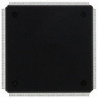
MCF5307AI90B Freescale Semiconductor, MCF5307AI90B Datasheet - Page 148

MCF5307AI90B
Manufacturer Part Number
MCF5307AI90B
Description
IC MPU 32BIT COLDF 90MHZ 208FQFP
Manufacturer
Freescale Semiconductor
Series
MCF530xr
Datasheets
1.MCF5307AI66B.pdf
(484 pages)
2.MCF5307AI66B.pdf
(16 pages)
3.MCF5307AI66B.pdf
(2 pages)
Specifications of MCF5307AI90B
Core Processor
Coldfire V3
Core Size
32-Bit
Speed
90MHz
Connectivity
EBI/EMI, I²C, UART/USART
Peripherals
DMA, POR, WDT
Number Of I /o
16
Program Memory Type
ROMless
Ram Size
4K x 8
Voltage - Supply (vcc/vdd)
3 V ~ 3.6 V
Oscillator Type
External
Operating Temperature
0°C ~ 70°C
Package / Case
208-FQFP
Maximum Clock Frequency
90 MHz
Maximum Operating Temperature
+ 105 C
Mounting Style
SMD/SMT
Minimum Operating Temperature
0 C
Family Name
MCF5xxx
Device Core
ColdFire
Device Core Size
32b
Frequency (max)
90MHz
Instruction Set Architecture
RISC
Supply Voltage 1 (typ)
3.3V
Operating Temp Range
0C to 70C
Operating Temperature Classification
Commercial
Mounting
Surface Mount
Pin Count
208
Package Type
FQFP
Program Memory Size
8KB
Cpu Speed
90MHz
Embedded Interface Type
I2C, UART
Digital Ic Case Style
FQFP
No. Of Pins
208
Supply Voltage Range
3V To 3.6V
Rohs Compliant
Yes
Lead Free Status / RoHS Status
Lead free / RoHS Compliant
Eeprom Size
-
Program Memory Size
-
Data Converters
-
Lead Free Status / Rohs Status
Lead free / RoHS Compliant
Available stocks
Company
Part Number
Manufacturer
Quantity
Price
Company:
Part Number:
MCF5307AI90B
Manufacturer:
FREESCAL
Quantity:
153
Company:
Part Number:
MCF5307AI90B
Manufacturer:
Freescale Semiconductor
Quantity:
10 000
Part Number:
MCF5307AI90B
Manufacturer:
FREESCALE
Quantity:
20 000
- Current page: 148 of 484
- Download datasheet (6Mb)
1
2
Read A/D
register
Write A/D
register
Read
memory
location
Write
memory
location
Dump
memory
block
Fill memory
block
Resume
execution
No operation
Output the
current PC
Read control
register
Write control
register
Read debug
module
register
Write debug
module
register
Background Debug Mode (BDM)
Unassigned command opcodes are reserved by Motorola. All unused command formats
within any revision level perform a
5.5.3.1 ColdFire BDM Command Format
All ColdFire Family BDM commands include a 16-bit operation word followed by an
optional set of one or more extension words, as shown in Figure 5-16.
Command
5-20
General command effect and/or requirements on CPU operation:
- Halted. The CPU must be halted to perform this command.
- Steal. Command generates bus cycles that can be interleaved with bus accesses.
- Parallel. Command is executed in parallel with CPU activity.
0x4 is a three-bit field.
RAREG
RDREG
WAREG
WDREG
READ
WRITE
DUMP
FILL
GO
NOP
SYNC
RCREG
WCREG
RDMREG
WDMREG
Mnemonic
_
PC
/
/
Read the selected address or data register and
return the results through the serial interface.
Write the data operand to the specified address or
data register.
Read the data at the memory location specified by
the longword address.
Write the operand data to the memory location
specified by the longword address.
Used with
An initial
address of the block and to retrieve the first result.
A
Used with
initial
address of the block and to supply the first operand.
A
The pipeline is flushed and refilled before resuming
instruction execution at the current PC.
Perform no operation; may be used as a null
command.
Capture the current PC and display it on the
PST/DDATA output pins.
Read the system control register.
Write the operand data to the system control
register.
Read the debug module register.
Write the operand data to the debug module
register.
DUMP
FILL
Freescale Semiconductor, Inc.
Table 5-17. BDM Command Summary
WRITE
command writes subsequent operands.
For More Information On This Product,
command retrieves subsequent operands.
READ
READ
WRITE
is executed to set up the starting
is executed to set up the starting
to dump large blocks of memory.
Go to: www.freescale.com
to fill large blocks of memory. An
MCF5307 User’s Manual
Description
NOP
and return the illegal command response.
Parallel
Parallel
Parallel
Parallel
State
Halted
Halted
Halted
Halted
Halted
Steal
Steal
Steal
Steal
CPU
1
5.5.3.3.10 0x2980
5.5.3.3.11 0x2880
5.5.3.3.12 0x2D {0x4
5.5.3.3.13 0x2C {0x4
5.5.3.3.1 0x218 {A/D,
5.5.3.3.2 0x208 {A/D,
5.5.3.3.3 0x1900—byte
5.5.3.3.4 0x1800—byte
5.5.3.3.5 0x1D00—byte
5.5.3.3.6 0x1C00—byte
5.5.3.3.7 0x0C00
5.5.3.3.8 0x0000
5.5.3.3.9 0x0001
Section
Reg[2:0]}
Reg[2:0]}
0x1940—word
0x1980—lword
0x1840—word
0x1880—lword
0x1D40—word
0x1D80—lword
0x1C40—word
0x1C80—lword
DRc[4:0]}
Drc[4:0]}
Command
(Hex)
2
2
Related parts for MCF5307AI90B
Image
Part Number
Description
Manufacturer
Datasheet
Request
R
Part Number:
Description:
Manufacturer:
Freescale Semiconductor, Inc
Datasheet:
Part Number:
Description:
Mcf5307 Coldfire Integrated Microprocessor User
Manufacturer:
Freescale Semiconductor, Inc
Datasheet:
Part Number:
Description:
Manufacturer:
Freescale Semiconductor, Inc
Datasheet:
Part Number:
Description:
Manufacturer:
Freescale Semiconductor, Inc
Datasheet:
Part Number:
Description:
Manufacturer:
Freescale Semiconductor, Inc
Datasheet:
Part Number:
Description:
Manufacturer:
Freescale Semiconductor, Inc
Datasheet:
Part Number:
Description:
Manufacturer:
Freescale Semiconductor, Inc
Datasheet:
Part Number:
Description:
Manufacturer:
Freescale Semiconductor, Inc
Datasheet:
Part Number:
Description:
Manufacturer:
Freescale Semiconductor, Inc
Datasheet:
Part Number:
Description:
Manufacturer:
Freescale Semiconductor, Inc
Datasheet:
Part Number:
Description:
Manufacturer:
Freescale Semiconductor, Inc
Datasheet:
Part Number:
Description:
Manufacturer:
Freescale Semiconductor, Inc
Datasheet:
Part Number:
Description:
Manufacturer:
Freescale Semiconductor, Inc
Datasheet:
Part Number:
Description:
Manufacturer:
Freescale Semiconductor, Inc
Datasheet:
Part Number:
Description:
Manufacturer:
Freescale Semiconductor, Inc
Datasheet:


