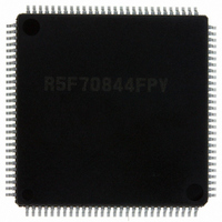
DF70844AD80FPV Renesas Electronics America, DF70844AD80FPV Datasheet - Page 901

DF70844AD80FPV
Manufacturer Part Number
DF70844AD80FPV
Description
IC SUPERH MCU FLASH 112LQFP
Manufacturer
Renesas Electronics America
Series
SuperH® SH7080r
Datasheet
1.DF70844AD80FPV.pdf
(1644 pages)
Specifications of DF70844AD80FPV
Core Size
32-Bit
Program Memory Size
256KB (256K x 8)
Core Processor
SH-2
Speed
80MHz
Connectivity
EBI/EMI, FIFO, I²C, SCI, SSU
Peripherals
DMA, POR, PWM, WDT
Number Of I /o
76
Program Memory Type
FLASH
Ram Size
16K x 8
Voltage - Supply (vcc/vdd)
3 V ~ 5.5 V
Data Converters
A/D 8x10b
Oscillator Type
Internal
Operating Temperature
-40°C ~ 85°C
Package / Case
112-LQFP
No. Of I/o's
76
Ram Memory Size
16KB
Cpu Speed
80MHz
Digital Ic Case Style
LQFP
Supply Voltage Range
3V To 3.6V, 4.5V To 5.5V
Embedded Interface Type
I2C, SCI
Rohs Compliant
Yes
Lead Free Status / RoHS Status
Lead free / RoHS Compliant
For Use With
R0K570865S001BE - KIT STARTER FOR SH7086R0K570865S000BE - KIT STARTER FOR SH7086HS0005KCU11H - EMULATOR E10A-USB H8S(X),SH2(A)
Eeprom Size
-
Lead Free Status / RoHS Status
Lead free / RoHS Compliant, Lead free / RoHS Compliant
Available stocks
Company
Part Number
Manufacturer
Quantity
Price
Company:
Part Number:
DF70844AD80FPV
Manufacturer:
Renesas Electronics America
Quantity:
10 000
- Current page: 901 of 1644
- Download datasheet (10Mb)
In clock synchronous serial communication, each data bit is output on the communication line
from one falling edge of the serial clock to the next. Data is guaranteed valid at the rising edge of
the serial clock. In each character, the serial data bits are transmitted in order from the LSB (first)
to the MSB (last). After output of the MSB, the communication line remains in the state of the
MSB. In clock synchronous mode, the SCIF receives data in synchronization with the rising edge
of the serial clock.
(1)
The data length is fixed at eight bits. No parity bit can be added.
(2)
An internal clock generated by the on-chip baud rate generator or an external clock input from the
SCK pin can be selected as the SCIF transmit/receive clock.
When the SCIF operates on an internal clock, it outputs the clock signal at the SCK pin. Eight
clock pulses are output per transmitted or received character. When the SCIF is not transmitting or
receiving, the clock signal remains in the high state. When only receiving, the clock signal outputs
while the RE bit of SCSCR is 1 and the number of data in receive FIFO is more than the receive
FIFO data trigger number. In this case, 8 × (16 + 1) = 136 pulses of synchronous clock are output.
To perform reception of n characters of data, select an external clock as the clock source. If an
internal clock should be used, set RE = 1 and TE = 1 and receive n characters of data
simultaneously with the transmission of n characters of dummy data.
(3)
SCIF Initialization (Clock Synchronous Mode): Before transmitting, receiving, or changing the
mode or communication format, the software must clear the TE and RE bits to 0 in the serial
control register (SCSCR), then initialize the SCIF. Clearing TE to 0 initializes the transmit shift
register (SCTSR). Clearing RE to 0, however, does not initialize the RDF, PER, FER, and ORER
flags and receive data register (SCRDR), which retain their previous contents.
Communication Format
Clock
Transmitting and Receiving Data
Section 16 Serial Communication Interface with FIFO (SCIF)
Rev. 3.00 May 17, 2007 Page 843 of 1582
REJ09B0181-0300
Related parts for DF70844AD80FPV
Image
Part Number
Description
Manufacturer
Datasheet
Request
R

Part Number:
Description:
KIT STARTER FOR M16C/29
Manufacturer:
Renesas Electronics America
Datasheet:

Part Number:
Description:
KIT STARTER FOR R8C/2D
Manufacturer:
Renesas Electronics America
Datasheet:

Part Number:
Description:
R0K33062P STARTER KIT
Manufacturer:
Renesas Electronics America
Datasheet:

Part Number:
Description:
KIT STARTER FOR R8C/23 E8A
Manufacturer:
Renesas Electronics America
Datasheet:

Part Number:
Description:
KIT STARTER FOR R8C/25
Manufacturer:
Renesas Electronics America
Datasheet:

Part Number:
Description:
KIT STARTER H8S2456 SHARPE DSPLY
Manufacturer:
Renesas Electronics America
Datasheet:

Part Number:
Description:
KIT STARTER FOR R8C38C
Manufacturer:
Renesas Electronics America
Datasheet:

Part Number:
Description:
KIT STARTER FOR R8C35C
Manufacturer:
Renesas Electronics America
Datasheet:

Part Number:
Description:
KIT STARTER FOR R8CL3AC+LCD APPS
Manufacturer:
Renesas Electronics America
Datasheet:

Part Number:
Description:
KIT STARTER FOR RX610
Manufacturer:
Renesas Electronics America
Datasheet:

Part Number:
Description:
KIT STARTER FOR R32C/118
Manufacturer:
Renesas Electronics America
Datasheet:

Part Number:
Description:
KIT DEV RSK-R8C/26-29
Manufacturer:
Renesas Electronics America
Datasheet:

Part Number:
Description:
KIT STARTER FOR SH7124
Manufacturer:
Renesas Electronics America
Datasheet:

Part Number:
Description:
KIT STARTER FOR H8SX/1622
Manufacturer:
Renesas Electronics America
Datasheet:

Part Number:
Description:
KIT DEV FOR SH7203
Manufacturer:
Renesas Electronics America
Datasheet:


