DF70844AD80FPV Renesas Electronics America, DF70844AD80FPV Datasheet - Page 1298
DF70844AD80FPV
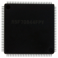
Manufacturer Part Number
DF70844AD80FPV
Description
IC SUPERH MCU FLASH 112LQFP
Manufacturer
Renesas Electronics America
Series
SuperH® SH7080r
Datasheet
1.DF70844AD80FPV.pdf
(1644 pages)
Specifications of DF70844AD80FPV
Core Size
32-Bit
Program Memory Size
256KB (256K x 8)
Core Processor
SH-2
Speed
80MHz
Connectivity
EBI/EMI, FIFO, I²C, SCI, SSU
Peripherals
DMA, POR, PWM, WDT
Number Of I /o
76
Program Memory Type
FLASH
Ram Size
16K x 8
Voltage - Supply (vcc/vdd)
3 V ~ 5.5 V
Data Converters
A/D 8x10b
Oscillator Type
Internal
Operating Temperature
-40°C ~ 85°C
Package / Case
112-LQFP
No. Of I/o's
76
Ram Memory Size
16KB
Cpu Speed
80MHz
Digital Ic Case Style
LQFP
Supply Voltage Range
3V To 3.6V, 4.5V To 5.5V
Embedded Interface Type
I2C, SCI
Rohs Compliant
Yes
Lead Free Status / RoHS Status
Lead free / RoHS Compliant
For Use With
R0K570865S001BE - KIT STARTER FOR SH7086R0K570865S000BE - KIT STARTER FOR SH7086HS0005KCU11H - EMULATOR E10A-USB H8S(X),SH2(A)
Eeprom Size
-
Lead Free Status / RoHS Status
Lead free / RoHS Compliant, Lead free / RoHS Compliant
Available stocks
Company
Part Number
Manufacturer
Quantity
Price
Company:

Part Number:
DF70844AD80FPV
Manufacturer:
Renesas Electronics America
Quantity:
10 000


Section 23 Flash Memory
Rev. 3.00 May 17, 2007 Page 1240 of 1582
REJ09B0181-0300
Bit
31 to 0 UA31 to
Bit Name
UA0
Initial
Value
Undefined R/W
R/W
Description
User Branch Destination Address
When the user branch is not required, address 0
(H'00000000) must be set.
The user branch destination must be an area other than
the flash memory, an area other than the RAM area in
which on-chip program has been transferred, or the
external bus space.
Note that the CPU must not branch to an area without
the execution code and get out of control. The on-chip
program download area and stack area must not be
overwritten. If CPU runaway occurs or the download
area or stack area is overwritten, the value of flash
memory cannot be guaranteed.
The download of the on-chip program, initialization,
initiation of the programming/erasing program must not
be executed in the processing of the user branch
destination. Programming or erasing cannot be
guaranteed when returning from the user branch
destination. The program data which has already been
prepared must not be programmed.
Store general registers R8 to R15. General registers R0
to R7 are available without storing them.
Moreover, the programming/erasing interface registers
must not be written to or RAM emulation mode must not
be entered in the processing of the user branch
destination.
After the processing of the user branch has ended, the
programming/erasing program must be returned to by
using the RTS instruction.
For the execution intervals of the user branch
processing, see note 2 (User branch processing
intervals) in section 23.8.3, Other Notes.
Related parts for DF70844AD80FPV
Image
Part Number
Description
Manufacturer
Datasheet
Request
R

Part Number:
Description:
KIT STARTER FOR M16C/29
Manufacturer:
Renesas Electronics America
Datasheet:

Part Number:
Description:
KIT STARTER FOR R8C/2D
Manufacturer:
Renesas Electronics America
Datasheet:

Part Number:
Description:
R0K33062P STARTER KIT
Manufacturer:
Renesas Electronics America
Datasheet:

Part Number:
Description:
KIT STARTER FOR R8C/23 E8A
Manufacturer:
Renesas Electronics America
Datasheet:

Part Number:
Description:
KIT STARTER FOR R8C/25
Manufacturer:
Renesas Electronics America
Datasheet:

Part Number:
Description:
KIT STARTER H8S2456 SHARPE DSPLY
Manufacturer:
Renesas Electronics America
Datasheet:

Part Number:
Description:
KIT STARTER FOR R8C38C
Manufacturer:
Renesas Electronics America
Datasheet:

Part Number:
Description:
KIT STARTER FOR R8C35C
Manufacturer:
Renesas Electronics America
Datasheet:

Part Number:
Description:
KIT STARTER FOR R8CL3AC+LCD APPS
Manufacturer:
Renesas Electronics America
Datasheet:
Part Number:
Description:
KIT STARTER FOR RX610
Manufacturer:
Renesas Electronics America
Datasheet:

Part Number:
Description:
KIT STARTER FOR R32C/118
Manufacturer:
Renesas Electronics America
Datasheet:

Part Number:
Description:
KIT DEV RSK-R8C/26-29
Manufacturer:
Renesas Electronics America
Datasheet:

Part Number:
Description:
KIT STARTER FOR SH7124
Manufacturer:
Renesas Electronics America
Datasheet:

Part Number:
Description:
KIT STARTER FOR H8SX/1622
Manufacturer:
Renesas Electronics America
Datasheet:

Part Number:
Description:
KIT DEV FOR SH7203
Manufacturer:
Renesas Electronics America
Datasheet: