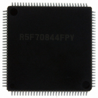
DF70844AD80FPV Renesas Electronics America, DF70844AD80FPV Datasheet - Page 832

DF70844AD80FPV
Manufacturer Part Number
DF70844AD80FPV
Description
IC SUPERH MCU FLASH 112LQFP
Manufacturer
Renesas Electronics America
Series
SuperH® SH7080r
Datasheet
1.DF70844AD80FPV.pdf
(1644 pages)
Specifications of DF70844AD80FPV
Core Size
32-Bit
Program Memory Size
256KB (256K x 8)
Core Processor
SH-2
Speed
80MHz
Connectivity
EBI/EMI, FIFO, I²C, SCI, SSU
Peripherals
DMA, POR, PWM, WDT
Number Of I /o
76
Program Memory Type
FLASH
Ram Size
16K x 8
Voltage - Supply (vcc/vdd)
3 V ~ 5.5 V
Data Converters
A/D 8x10b
Oscillator Type
Internal
Operating Temperature
-40°C ~ 85°C
Package / Case
112-LQFP
No. Of I/o's
76
Ram Memory Size
16KB
Cpu Speed
80MHz
Digital Ic Case Style
LQFP
Supply Voltage Range
3V To 3.6V, 4.5V To 5.5V
Embedded Interface Type
I2C, SCI
Rohs Compliant
Yes
Lead Free Status / RoHS Status
Lead free / RoHS Compliant
For Use With
R0K570865S001BE - KIT STARTER FOR SH7086R0K570865S000BE - KIT STARTER FOR SH7086HS0005KCU11H - EMULATOR E10A-USB H8S(X),SH2(A)
Eeprom Size
-
Lead Free Status / RoHS Status
Lead free / RoHS Compliant, Lead free / RoHS Compliant
Available stocks
Company
Part Number
Manufacturer
Quantity
Price
Company:
Part Number:
DF70844AD80FPV
Manufacturer:
Renesas Electronics America
Quantity:
10 000
- Current page: 832 of 1644
- Download datasheet (10Mb)
Section 15 Serial Communication Interface (SCI)
Rev. 3.00 May 17, 2007 Page 774 of 1582
REJ09B0181-0300
Note:
No
No
No
When switching from transmit or receive operation to simultaneous transmit and receive operations, first clear the
TE bit and RE bit to 0, then set both these bits to 1 simultaneously.
Clear TE and RE bits in SCSCR to 0
Start of transmission and reception
Write transmit data to SCTDR, and
Figure 15.14 Sample Flowchart for Transmitting/Receiving Serial Data
Write transmit data to SCTDR and
End of transmission and reception
clear TDRE flag in SCSSR to 0
clear TDRE flag in SCSSR to 0
Read ORER flag in SCSSR
Read TDRE flag in SCSSR
Read RDRF flag in SCSSR
All data received?
ORER = 1?
TDRE = 1?
RDRF = 1?
Yes
Yes
Yes
No
Error processing
Yes
[1]
[2]
[3]
[4]
SCI status check and transmit data write:
Read SCSSR and check that the TDRE flag is
set to 1, then write transmit data to SCTDR and
clear the TDRE flag to 0.
Transition of the TDRE flag from 0 to 1 can also
be identified by a TXI interrupt.
Receive error processing:
If a receive error occurs, read the ORER flag in
SCSSR, and after performing the appropriate
error processing, clear the ORER flag to 0.
Reception cannot be resumed if the ORER flag
is set to 1.
SCI status check and receive data read:
Read SCSSR and check that the RDRF flag is
set to 1, then read the receive data in SCRDR
and clear the RDRF flag to 0. Transition of the
RDRF flag from 0 to 1 can also be identified by
an RXI interrupt.
Serial transmission/reception continuation
procedure:
To continue serial transmission/reception,
before the MSB (bit 7) of the current frame is
received, finish reading the RDRF flag, reading
SCRDR, and clearing the RDRF flag to 0. Also,
before the MSB (bit 7) of the current frame is
transmitted, read 1 from the TDRE flag to
confirm that writing is possible. Then write data
to SCTDR and clear the TDRE flag to 0.
Checking and clearing of the TDRE flag is
automatic when the DTC or DMAC is activated
by a transmit data empty interrupt (TXI) request
and data is written to SCTDR. Also, the RDRF
flag is cleared automatically when the DTC or
DMAC is activated by a receive data full
interrupt (RXI) request and the SCRDR value is
read.
Related parts for DF70844AD80FPV
Image
Part Number
Description
Manufacturer
Datasheet
Request
R

Part Number:
Description:
KIT STARTER FOR M16C/29
Manufacturer:
Renesas Electronics America
Datasheet:

Part Number:
Description:
KIT STARTER FOR R8C/2D
Manufacturer:
Renesas Electronics America
Datasheet:

Part Number:
Description:
R0K33062P STARTER KIT
Manufacturer:
Renesas Electronics America
Datasheet:

Part Number:
Description:
KIT STARTER FOR R8C/23 E8A
Manufacturer:
Renesas Electronics America
Datasheet:

Part Number:
Description:
KIT STARTER FOR R8C/25
Manufacturer:
Renesas Electronics America
Datasheet:

Part Number:
Description:
KIT STARTER H8S2456 SHARPE DSPLY
Manufacturer:
Renesas Electronics America
Datasheet:

Part Number:
Description:
KIT STARTER FOR R8C38C
Manufacturer:
Renesas Electronics America
Datasheet:

Part Number:
Description:
KIT STARTER FOR R8C35C
Manufacturer:
Renesas Electronics America
Datasheet:

Part Number:
Description:
KIT STARTER FOR R8CL3AC+LCD APPS
Manufacturer:
Renesas Electronics America
Datasheet:

Part Number:
Description:
KIT STARTER FOR RX610
Manufacturer:
Renesas Electronics America
Datasheet:

Part Number:
Description:
KIT STARTER FOR R32C/118
Manufacturer:
Renesas Electronics America
Datasheet:

Part Number:
Description:
KIT DEV RSK-R8C/26-29
Manufacturer:
Renesas Electronics America
Datasheet:

Part Number:
Description:
KIT STARTER FOR SH7124
Manufacturer:
Renesas Electronics America
Datasheet:

Part Number:
Description:
KIT STARTER FOR H8SX/1622
Manufacturer:
Renesas Electronics America
Datasheet:

Part Number:
Description:
KIT DEV FOR SH7203
Manufacturer:
Renesas Electronics America
Datasheet:


