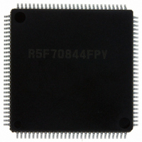
DF70844AD80FPV Renesas Electronics America, DF70844AD80FPV Datasheet - Page 39

DF70844AD80FPV
Manufacturer Part Number
DF70844AD80FPV
Description
IC SUPERH MCU FLASH 112LQFP
Manufacturer
Renesas Electronics America
Series
SuperH® SH7080r
Datasheet
1.DF70844AD80FPV.pdf
(1644 pages)
Specifications of DF70844AD80FPV
Core Size
32-Bit
Program Memory Size
256KB (256K x 8)
Core Processor
SH-2
Speed
80MHz
Connectivity
EBI/EMI, FIFO, I²C, SCI, SSU
Peripherals
DMA, POR, PWM, WDT
Number Of I /o
76
Program Memory Type
FLASH
Ram Size
16K x 8
Voltage - Supply (vcc/vdd)
3 V ~ 5.5 V
Data Converters
A/D 8x10b
Oscillator Type
Internal
Operating Temperature
-40°C ~ 85°C
Package / Case
112-LQFP
No. Of I/o's
76
Ram Memory Size
16KB
Cpu Speed
80MHz
Digital Ic Case Style
LQFP
Supply Voltage Range
3V To 3.6V, 4.5V To 5.5V
Embedded Interface Type
I2C, SCI
Rohs Compliant
Yes
Lead Free Status / RoHS Status
Lead free / RoHS Compliant
For Use With
R0K570865S001BE - KIT STARTER FOR SH7086R0K570865S000BE - KIT STARTER FOR SH7086HS0005KCU11H - EMULATOR E10A-USB H8S(X),SH2(A)
Eeprom Size
-
Lead Free Status / RoHS Status
Lead free / RoHS Compliant, Lead free / RoHS Compliant
Available stocks
Company
Part Number
Manufacturer
Quantity
Price
Company:
Part Number:
DF70844AD80FPV
Manufacturer:
Renesas Electronics America
Quantity:
10 000
- Current page: 39 of 1644
- Download datasheet (10Mb)
Section 16 Serial Communication Interface with FIFO (SCIF)
Figure 16.1 Block Diagram of SCIF........................................................................................... 790
Figure 16.2 Example of Data Format in Asynchronous Communication
(8-Bit Data with Parity and Two Stop Bits) ............................................................ 831
Figure 16.3 Sample Flowchart for SCIF Initialization ............................................................... 834
Figure 16.4 Sample Flowchart for Transmitting Serial Data ...................................................... 835
Figure 16.5 Example of Transmit Operation (8-Bit Data, Parity, One Stop Bit)........................ 837
Figure 16.6 Example of Operation Using Modem Control (CTS).............................................. 837
Figure 16.7 Sample Flowchart for Receiving Serial Data .......................................................... 838
Figure 16.8 Sample Flowchart for Receiving Serial Data (cont)................................................ 839
Figure 16.9 Example of SCIF Receive Operation (8-Bit Data, Parity, One Stop Bit)................ 841
Figure 16.10 Example of Operation Using Modem Control (RTS)............................................ 841
Figure 16.11 Data Format in Clock Synchronous Communication ............................................ 842
Figure 16.12 Sample Flowchart for SCIF Initialization.............................................................. 844
Figure 16.13 Sample Flowchart for Transmitting Serial Data .................................................... 845
Figure 16.14 Example of SCIF Transmit Operation................................................................... 846
Figure 16.15 Sample Flowchart for Receiving Serial Data (1)................................................... 847
Figure 16.16 Sample Flowchart for Receiving Serial Data (2)................................................... 848
Figure 16.17 Example of SCIF Receive Operation .................................................................... 848
Figure 16.18 Sample Flowchart for Transmitting/Receiving Serial Data................................... 849
Figure 16.19 RTSIO Bit, RTSDT Bit, and RTS Pin................................................................... 851
Figure 16.20 CTSIO Bit, CTSDT bit, and CTS Pin ................................................................... 852
Figure 16.21 SCKIO Bit, SCKDT bit, and SCK Pin .................................................................. 852
Figure 16.22 SPBIO Bit, SPBDT bit, and TXD Pin ................................................................... 853
Figure 16.23 Receive Data Sampling Timing in Asynchronous Mode ...................................... 856
Section 17 Synchronous Serial Communication Unit (SSU)
Figure 17.1 Block Diagram of SSU............................................................................................ 860
Figure 17.2 Relationship of Clock Phase, Polarity, and Data..................................................... 876
Figure 17.3 Relationship between Data Input/Output Pins and the Shift Register ..................... 878
Figure 17.4 Example of Initial Settings in SSU Mode ............................................................... 882
Figure 17.5 Example of Transmission Operation (SSU Mode) .................................................. 884
Figure 17.6 Flowchart Example of Data Transmission (SSU Mode) ......................................... 885
Figure 17.7 Example of Reception Operation (SSU Mode) ....................................................... 887
Figure 17.8 Flowchart Example of Data Reception (SSU Mode)............................................... 888
Figure 17.9 Flowchart Example of Simultaneous Transmission/Reception (SSU Mode) .......... 889
Figure 17.10 Conflict Error Detection Timing (Before Transfer) .............................................. 890
Figure 17.11 Conflict Error Detection Timing (After Transfer End) ......................................... 891
Figure 17.12 Example of Initial Settings in Clock Synchronous Communication Mode ........... 892
Rev. 3.00 May 17, 2007 Page xxxix of Iviii
Related parts for DF70844AD80FPV
Image
Part Number
Description
Manufacturer
Datasheet
Request
R

Part Number:
Description:
KIT STARTER FOR M16C/29
Manufacturer:
Renesas Electronics America
Datasheet:

Part Number:
Description:
KIT STARTER FOR R8C/2D
Manufacturer:
Renesas Electronics America
Datasheet:

Part Number:
Description:
R0K33062P STARTER KIT
Manufacturer:
Renesas Electronics America
Datasheet:

Part Number:
Description:
KIT STARTER FOR R8C/23 E8A
Manufacturer:
Renesas Electronics America
Datasheet:

Part Number:
Description:
KIT STARTER FOR R8C/25
Manufacturer:
Renesas Electronics America
Datasheet:

Part Number:
Description:
KIT STARTER H8S2456 SHARPE DSPLY
Manufacturer:
Renesas Electronics America
Datasheet:

Part Number:
Description:
KIT STARTER FOR R8C38C
Manufacturer:
Renesas Electronics America
Datasheet:

Part Number:
Description:
KIT STARTER FOR R8C35C
Manufacturer:
Renesas Electronics America
Datasheet:

Part Number:
Description:
KIT STARTER FOR R8CL3AC+LCD APPS
Manufacturer:
Renesas Electronics America
Datasheet:

Part Number:
Description:
KIT STARTER FOR RX610
Manufacturer:
Renesas Electronics America
Datasheet:

Part Number:
Description:
KIT STARTER FOR R32C/118
Manufacturer:
Renesas Electronics America
Datasheet:

Part Number:
Description:
KIT DEV RSK-R8C/26-29
Manufacturer:
Renesas Electronics America
Datasheet:

Part Number:
Description:
KIT STARTER FOR SH7124
Manufacturer:
Renesas Electronics America
Datasheet:

Part Number:
Description:
KIT STARTER FOR H8SX/1622
Manufacturer:
Renesas Electronics America
Datasheet:

Part Number:
Description:
KIT DEV FOR SH7203
Manufacturer:
Renesas Electronics America
Datasheet:


