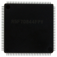
DF70844AD80FPV Renesas Electronics America, DF70844AD80FPV Datasheet - Page 859

DF70844AD80FPV
Manufacturer Part Number
DF70844AD80FPV
Description
IC SUPERH MCU FLASH 112LQFP
Manufacturer
Renesas Electronics America
Series
SuperH® SH7080r
Datasheet
1.DF70844AD80FPV.pdf
(1644 pages)
Specifications of DF70844AD80FPV
Core Size
32-Bit
Program Memory Size
256KB (256K x 8)
Core Processor
SH-2
Speed
80MHz
Connectivity
EBI/EMI, FIFO, I²C, SCI, SSU
Peripherals
DMA, POR, PWM, WDT
Number Of I /o
76
Program Memory Type
FLASH
Ram Size
16K x 8
Voltage - Supply (vcc/vdd)
3 V ~ 5.5 V
Data Converters
A/D 8x10b
Oscillator Type
Internal
Operating Temperature
-40°C ~ 85°C
Package / Case
112-LQFP
No. Of I/o's
76
Ram Memory Size
16KB
Cpu Speed
80MHz
Digital Ic Case Style
LQFP
Supply Voltage Range
3V To 3.6V, 4.5V To 5.5V
Embedded Interface Type
I2C, SCI
Rohs Compliant
Yes
Lead Free Status / RoHS Status
Lead free / RoHS Compliant
For Use With
R0K570865S001BE - KIT STARTER FOR SH7086R0K570865S000BE - KIT STARTER FOR SH7086HS0005KCU11H - EMULATOR E10A-USB H8S(X),SH2(A)
Eeprom Size
-
Lead Free Status / RoHS Status
Lead free / RoHS Compliant, Lead free / RoHS Compliant
Available stocks
Company
Part Number
Manufacturer
Quantity
Price
Company:
Part Number:
DF70844AD80FPV
Manufacturer:
Renesas Electronics America
Quantity:
10 000
- Current page: 859 of 1644
- Download datasheet (10Mb)
Bit
2
1, 0
Bit Name
CKE[1:0]
Initial
value
0
00
R/W
R
R/W
Description
Reserved
This bit is always read as 0. The write value should
always be 0.
Clock Enable 1 and 0
Select the SCIF clock source and enable or disable
clock output from the SCK pin. Depending on the
combination of CKE1 and CKE0, the SCK pin can be
used for serial clock output or serial clock input.
The CKE0 setting is valid only when the SCIF is
operating on the internal clock (CKE1 = 0). The CKE0
setting is ignored when an external clock source is
selected (CKE1 = 1). In clock synchronous mode, select
the SCIF operating mode in the serial mode register
(SCSMR), then set CKE1 and CKE0.
•
00: Internal clock, SCK pin used for input pin (The input
01: Internal clock, SCK pin used for clock output
10: External clock, SCK pin used for clock input
11: Setting prohibited
•
00: Internal clock, SCK pin used for serial clock output
01: Internal clock, SCK pin used for serial clock output
10: External clock, SCK pin used for serial clock input
11: Setting prohibited
Section 16 Serial Communication Interface with FIFO (SCIF)
Asynchronous mode
Clock synchronous mode
signal is ignored. The state of the SCK pin depends
on both the SCKIO and SCKDT bits.)
(The output clock frequency is 16 times the bit rate.)
(The input clock frequency is 16 times the bit rate.)
Rev. 3.00 May 17, 2007 Page 801 of 1582
REJ09B0181-0300
Related parts for DF70844AD80FPV
Image
Part Number
Description
Manufacturer
Datasheet
Request
R

Part Number:
Description:
KIT STARTER FOR M16C/29
Manufacturer:
Renesas Electronics America
Datasheet:

Part Number:
Description:
KIT STARTER FOR R8C/2D
Manufacturer:
Renesas Electronics America
Datasheet:

Part Number:
Description:
R0K33062P STARTER KIT
Manufacturer:
Renesas Electronics America
Datasheet:

Part Number:
Description:
KIT STARTER FOR R8C/23 E8A
Manufacturer:
Renesas Electronics America
Datasheet:

Part Number:
Description:
KIT STARTER FOR R8C/25
Manufacturer:
Renesas Electronics America
Datasheet:

Part Number:
Description:
KIT STARTER H8S2456 SHARPE DSPLY
Manufacturer:
Renesas Electronics America
Datasheet:

Part Number:
Description:
KIT STARTER FOR R8C38C
Manufacturer:
Renesas Electronics America
Datasheet:

Part Number:
Description:
KIT STARTER FOR R8C35C
Manufacturer:
Renesas Electronics America
Datasheet:

Part Number:
Description:
KIT STARTER FOR R8CL3AC+LCD APPS
Manufacturer:
Renesas Electronics America
Datasheet:

Part Number:
Description:
KIT STARTER FOR RX610
Manufacturer:
Renesas Electronics America
Datasheet:

Part Number:
Description:
KIT STARTER FOR R32C/118
Manufacturer:
Renesas Electronics America
Datasheet:

Part Number:
Description:
KIT DEV RSK-R8C/26-29
Manufacturer:
Renesas Electronics America
Datasheet:

Part Number:
Description:
KIT STARTER FOR SH7124
Manufacturer:
Renesas Electronics America
Datasheet:

Part Number:
Description:
KIT STARTER FOR H8SX/1622
Manufacturer:
Renesas Electronics America
Datasheet:

Part Number:
Description:
KIT DEV FOR SH7203
Manufacturer:
Renesas Electronics America
Datasheet:


