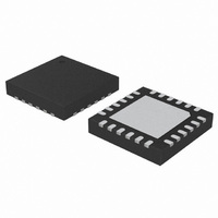
C8051F902-GM Silicon Laboratories Inc, C8051F902-GM Datasheet - Page 86

C8051F902-GM
Manufacturer Part Number
C8051F902-GM
Description
IC MCU 8BIT 8KB FLASH 24QFN
Manufacturer
Silicon Laboratories Inc
Series
C8051F9xxr
Specifications of C8051F902-GM
Program Memory Type
FLASH
Program Memory Size
8KB (8K x 8)
Package / Case
24-QFN
Core Processor
8051
Core Size
8-Bit
Speed
25MHz
Connectivity
SMBus (2-Wire/I²C), SPI, UART/USART
Peripherals
Brown-out Detect/Reset, POR, PWM, Temp Sensor, WDT
Number Of I /o
16
Ram Size
768 x 8
Voltage - Supply (vcc/vdd)
0.9 V ~ 3.6 V
Data Converters
A/D 15x10/12b
Oscillator Type
Internal
Operating Temperature
-40°C ~ 85°C
Processor Series
C8051F9x
Core
8051
Data Ram Size
768 B
Interface Type
UART
Maximum Clock Frequency
25 MHz
Number Of Timers
4
Operating Supply Voltage
0.9 V to 3.6 V
Maximum Operating Temperature
+ 85 C
Mounting Style
SMD/SMT
3rd Party Development Tools
PK51, CA51, A51, ULINK2
Development Tools By Supplier
C8051F912DK
Minimum Operating Temperature
- 40 C
On-chip Adc
12 bit
Package
24QFN EP
Device Core
8051
Family Name
C8051F90x
Maximum Speed
25 MHz
Data Bus Width
8 Bit
Number Of Programmable I/os
16
Lead Free Status / RoHS Status
Lead free / RoHS Compliant
Eeprom Size
-
Lead Free Status / Rohs Status
Lead free / RoHS Compliant
Other names
336-1848-5
- Current page: 86 of 318
- Download datasheet (3Mb)
C8051F91x-C8051F90x
6.
C8051F91x-C8051F90x devices include an on-chip programmable current reference (source or sink) with
two output current settings: Low Power Mode and High Current Mode. The maximum current output in Low
Power Mode is 63 µA (1 µA steps) and the maximum current output in High Current Mode is 504 µA (8 µA
steps).
The current source/sink is controlled though the IREF0CN special function register. It is enabled by setting
the desired output current to a non-zero value. It is disabled by writing 0x00 to IREF0CN. The port I/O pin
associated with ISRC0 should be configured as an analog input and skipped in the Crossbar. See Section
“21. Port Input/Output” on page 205 for more details.
SFR Definition 6.1. IREF0CN: Current Reference Control
SFR Page = 0x0; SFR Address = 0xB9
6.1.
On ‘F912 and ‘F902 devices, the precision of the current reference can be increased by fine tuning the
IREF0 output using a PWM signal generated by the PCA. This mode allows the IREF0DAT bits to perform
a course adjustment on the IREF0 output. Any available PCA channel can perform a fine adjustment on
the IREF0 output. When enabled (PWMEN = 1), the CEX signal selected using the PWMSS bit field is
internally routed to IREF0 to control the on time of a current source having the weight of 2 LSBs. With the
two least significant bits of IREF0DAT set to 00b, applying a 100% duty cycle on the CEX signal will be
equivalent to setting the two LSBs of IREF0DAT to 10b. PWM enhanced mode is enabled and setup using
the IREF0CF register.
86
Name
Reset
Type
Bit
5:0
7
6
Bit
Programmable Current Reference (IREF0)
IREF0DAT[5:0] IREF0 Data Word.
PWM Enhanced Mode
MDSEL
SINK
R/W
Name
SINK
7
0
MODE
R/W
IREF0 Current Sink Enable.
Selects if IREF0 is a current source or a current sink.
0: IREF0 is a current source.
1: IREF0 is a current sink.
IREF0 Output Mode Select.
Selects Low Power or High Current Mode.
0: Low Power Mode is selected (step size = 1 µA).
1: High Current Mode is selected (step size = 8 µA).
Specifies the number of steps required to achieve the desired output current.
Output current = direction x step size x IREF0DAT.
IREF0 is in a low power state when IREF0DAT is set to 0x00.
6
0
5
0
Rev. 1.0
4
0
Function
3
0
IREF0DAT
R/W
2
0
1
0
0
0
Related parts for C8051F902-GM
Image
Part Number
Description
Manufacturer
Datasheet
Request
R
Part Number:
Description:
SMD/C°/SINGLE-ENDED OUTPUT SILICON OSCILLATOR
Manufacturer:
Silicon Laboratories Inc
Part Number:
Description:
Manufacturer:
Silicon Laboratories Inc
Datasheet:
Part Number:
Description:
N/A N/A/SI4010 AES KEYFOB DEMO WITH LCD RX
Manufacturer:
Silicon Laboratories Inc
Datasheet:
Part Number:
Description:
N/A N/A/SI4010 SIMPLIFIED KEY FOB DEMO WITH LED RX
Manufacturer:
Silicon Laboratories Inc
Datasheet:
Part Number:
Description:
N/A/-40 TO 85 OC/EZLINK MODULE; F930/4432 HIGH BAND (REV E/B1)
Manufacturer:
Silicon Laboratories Inc
Part Number:
Description:
EZLink Module; F930/4432 Low Band (rev e/B1)
Manufacturer:
Silicon Laboratories Inc
Part Number:
Description:
I°/4460 10 DBM RADIO TEST CARD 434 MHZ
Manufacturer:
Silicon Laboratories Inc
Part Number:
Description:
I°/4461 14 DBM RADIO TEST CARD 868 MHZ
Manufacturer:
Silicon Laboratories Inc
Part Number:
Description:
I°/4463 20 DBM RFSWITCH RADIO TEST CARD 460 MHZ
Manufacturer:
Silicon Laboratories Inc
Part Number:
Description:
I°/4463 20 DBM RADIO TEST CARD 868 MHZ
Manufacturer:
Silicon Laboratories Inc
Part Number:
Description:
I°/4463 27 DBM RADIO TEST CARD 868 MHZ
Manufacturer:
Silicon Laboratories Inc
Part Number:
Description:
I°/4463 SKYWORKS 30 DBM RADIO TEST CARD 915 MHZ
Manufacturer:
Silicon Laboratories Inc
Part Number:
Description:
N/A N/A/-40 TO 85 OC/4463 RFMD 30 DBM RADIO TEST CARD 915 MHZ
Manufacturer:
Silicon Laboratories Inc
Part Number:
Description:
I°/4463 20 DBM RADIO TEST CARD 169 MHZ
Manufacturer:
Silicon Laboratories Inc


