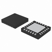
C8051F902-GM Silicon Laboratories Inc, C8051F902-GM Datasheet - Page 40

C8051F902-GM
Manufacturer Part Number
C8051F902-GM
Description
IC MCU 8BIT 8KB FLASH 24QFN
Manufacturer
Silicon Laboratories Inc
Series
C8051F9xxr
Specifications of C8051F902-GM
Program Memory Type
FLASH
Program Memory Size
8KB (8K x 8)
Package / Case
24-QFN
Core Processor
8051
Core Size
8-Bit
Speed
25MHz
Connectivity
SMBus (2-Wire/I²C), SPI, UART/USART
Peripherals
Brown-out Detect/Reset, POR, PWM, Temp Sensor, WDT
Number Of I /o
16
Ram Size
768 x 8
Voltage - Supply (vcc/vdd)
0.9 V ~ 3.6 V
Data Converters
A/D 15x10/12b
Oscillator Type
Internal
Operating Temperature
-40°C ~ 85°C
Processor Series
C8051F9x
Core
8051
Data Ram Size
768 B
Interface Type
UART
Maximum Clock Frequency
25 MHz
Number Of Timers
4
Operating Supply Voltage
0.9 V to 3.6 V
Maximum Operating Temperature
+ 85 C
Mounting Style
SMD/SMT
3rd Party Development Tools
PK51, CA51, A51, ULINK2
Development Tools By Supplier
C8051F912DK
Minimum Operating Temperature
- 40 C
On-chip Adc
12 bit
Package
24QFN EP
Device Core
8051
Family Name
C8051F90x
Maximum Speed
25 MHz
Data Bus Width
8 Bit
Number Of Programmable I/os
16
Lead Free Status / RoHS Status
Lead free / RoHS Compliant
Eeprom Size
-
Lead Free Status / Rohs Status
Lead free / RoHS Compliant
Other names
336-1848-5
- Current page: 40 of 318
- Download datasheet (3Mb)
C8051F91x-C8051F90x
Table 4.2. Global Electrical Characteristics (Continued)
–40 to +85 °C, 25 MHz system clock unless otherwise specified. See "AN358: Optimizing Low Power Operation of the
‘F9xx" for details on how to achieve the supply current specifications listed in this table.
40
Notes:
1. Based on device characterization data; Not production tested.
2. SYSCLK must be at least 32 kHz to enable debugging.
3. Digital Supply Current depends upon the particular code being executed. The values in this table are obtained
4. Includes oscillator and regulator supply current.
5. IDD can be estimated for frequencies <14 MHz by simply multiplying the frequency of interest by the
6. The supply current specifications in Table 4.2 are for two cell mode. The VBAT current in one-cell mode can
7. Idle IDD can be estimated by taking the current at 25 MHz minus the difference in current indicated by the
8. Internal LFO only available on ‘F912 and ‘F902 devices.
9. Ability to disable VBAT supply monitor only available on ‘F912 and ‘F902 devices.
with the CPU executing an “sjmp $” loop, which is the compiled form of a while(1) loop in C. One iteration
requires 3 CPU clock cycles, and the Flash memory is read on each cycle. The supply current will vary slightly
based on the physical location of the sjmp instruction and the number of Flash address lines that toggle as a
result. In the worst case, current can increase by up to 30% if the sjmp loop straddles a 64-byte Flash address
boundary (e.g., 0x007F to 0x0080). Real-world code with larger loops and longer linear sequences will have
few transitions across the 64-byte address boundaries.
frequency sensitivity number for that range, then adding an offset of 90 µA. When using these numbers to
estimate I
indicated by the frequency sensitivity number. For example: V
be estimated using the following equation:
The VBAT Voltage is the voltage at the VBAT pin, typically 0.9 to 1.8 V.
The Supply Current (two-cell mode) is the data sheet specification for supply current.
The Supply Voltage is the voltage at the VDD/DC+ pin, typically 1.8 to 3.3 V (default = 1.9 V).
The DC-DC Converter Efficiency can be estimated using Figure 4.3–Figure 4.5.
frequency sensitivity number. For example: V
(25 MHz – 20 MHz) x 0.102 mA/MHz = 3.5 mA assuming the same oscillator setting.
5 MHz) x 0.079 mA/MHz = 0.52 mA.
Parameter
VBAT Current (one-cell mode)
DD
for >14 MHz, the estimate should be the current at 25 MHz minus the difference in current
=
---------------------------------------------------------------------------------------------------------------------------------- -
Conditions
Supply Voltage Supply Current (two-cell mode)
DD
DC-DC Converter Efficiency VBAT Voltage
Rev. 1.0
= 3.0 V; F = 5 MHz, Idle I
DD
= 3.0 V; F = 20 MHz, I
DD
Min
= 2.1 mA – (25 MHz –
Typ
DD
= 4 mA –
Max
Units
Related parts for C8051F902-GM
Image
Part Number
Description
Manufacturer
Datasheet
Request
R
Part Number:
Description:
SMD/C°/SINGLE-ENDED OUTPUT SILICON OSCILLATOR
Manufacturer:
Silicon Laboratories Inc
Part Number:
Description:
Manufacturer:
Silicon Laboratories Inc
Datasheet:
Part Number:
Description:
N/A N/A/SI4010 AES KEYFOB DEMO WITH LCD RX
Manufacturer:
Silicon Laboratories Inc
Datasheet:
Part Number:
Description:
N/A N/A/SI4010 SIMPLIFIED KEY FOB DEMO WITH LED RX
Manufacturer:
Silicon Laboratories Inc
Datasheet:
Part Number:
Description:
N/A/-40 TO 85 OC/EZLINK MODULE; F930/4432 HIGH BAND (REV E/B1)
Manufacturer:
Silicon Laboratories Inc
Part Number:
Description:
EZLink Module; F930/4432 Low Band (rev e/B1)
Manufacturer:
Silicon Laboratories Inc
Part Number:
Description:
I°/4460 10 DBM RADIO TEST CARD 434 MHZ
Manufacturer:
Silicon Laboratories Inc
Part Number:
Description:
I°/4461 14 DBM RADIO TEST CARD 868 MHZ
Manufacturer:
Silicon Laboratories Inc
Part Number:
Description:
I°/4463 20 DBM RFSWITCH RADIO TEST CARD 460 MHZ
Manufacturer:
Silicon Laboratories Inc
Part Number:
Description:
I°/4463 20 DBM RADIO TEST CARD 868 MHZ
Manufacturer:
Silicon Laboratories Inc
Part Number:
Description:
I°/4463 27 DBM RADIO TEST CARD 868 MHZ
Manufacturer:
Silicon Laboratories Inc
Part Number:
Description:
I°/4463 SKYWORKS 30 DBM RADIO TEST CARD 915 MHZ
Manufacturer:
Silicon Laboratories Inc
Part Number:
Description:
N/A N/A/-40 TO 85 OC/4463 RFMD 30 DBM RADIO TEST CARD 915 MHZ
Manufacturer:
Silicon Laboratories Inc
Part Number:
Description:
I°/4463 20 DBM RADIO TEST CARD 169 MHZ
Manufacturer:
Silicon Laboratories Inc


