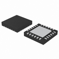
C8051F902-GM Silicon Laboratories Inc, C8051F902-GM Datasheet - Page 139

C8051F902-GM
Manufacturer Part Number
C8051F902-GM
Description
IC MCU 8BIT 8KB FLASH 24QFN
Manufacturer
Silicon Laboratories Inc
Series
C8051F9xxr
Specifications of C8051F902-GM
Program Memory Type
FLASH
Program Memory Size
8KB (8K x 8)
Package / Case
24-QFN
Core Processor
8051
Core Size
8-Bit
Speed
25MHz
Connectivity
SMBus (2-Wire/I²C), SPI, UART/USART
Peripherals
Brown-out Detect/Reset, POR, PWM, Temp Sensor, WDT
Number Of I /o
16
Ram Size
768 x 8
Voltage - Supply (vcc/vdd)
0.9 V ~ 3.6 V
Data Converters
A/D 15x10/12b
Oscillator Type
Internal
Operating Temperature
-40°C ~ 85°C
Processor Series
C8051F9x
Core
8051
Data Ram Size
768 B
Interface Type
UART
Maximum Clock Frequency
25 MHz
Number Of Timers
4
Operating Supply Voltage
0.9 V to 3.6 V
Maximum Operating Temperature
+ 85 C
Mounting Style
SMD/SMT
3rd Party Development Tools
PK51, CA51, A51, ULINK2
Development Tools By Supplier
C8051F912DK
Minimum Operating Temperature
- 40 C
On-chip Adc
12 bit
Package
24QFN EP
Device Core
8051
Family Name
C8051F90x
Maximum Speed
25 MHz
Data Bus Width
8 Bit
Number Of Programmable I/os
16
Lead Free Status / RoHS Status
Lead free / RoHS Compliant
Eeprom Size
-
Lead Free Status / Rohs Status
Lead free / RoHS Compliant
Other names
336-1848-5
- Current page: 139 of 318
- Download datasheet (3Mb)
13.6. Minimizing Flash Read Current
The Flash memory in the C8051F91x-C8051F90x devices is responsible for a substantial portion of the
total digital supply current when the device is executing code. Below are suggestions to minimize Flash
read current.
1. Use idle, suspend, or sleep modes while waiting for an interrupt, rather than polling the inter-
2. C8051F91x-C8051F90x devices have a one-shot timer that saves power when operating at
3. Flash read current depends on the number of address lines that toggle between sequential
rupt flag. Idle Mode is particularly well-suited for use in implementing short pauses, since the
wake-up time is no more than three system clock cycles. See the Power Management chapter
for details on the various low-power operating modes.
system clock frequencies of 14 MHz or less. The one-shot timer generates a minimum-dura-
tion enable signal for the Flash sense amps on each clock cycle in which the Flash memory is
accessed. This allows the Flash to remain in a low power state for the remainder of the long
clock cycle.
At clock frequencies above 14 MHz, the system clock cycle becomes short enough that the
one-shot timer no longer provides a power benefit. Disabling the one-shot timer at higher fre-
quencies reduces power consumption. The one-shot is enabled by default, and it can be dis-
abled (bypassed) by setting the BYPASS bit (FLSCL.6) to logic 1. To re-enable the one-shot,
clear the BYPASS bit to logic 0.
Flash read operations. In most cases, the difference in power is relatively small (on the order
of 5%).
The Flash memory is organized in rows of 64 bytes. A substantial current increase can be
detected when the read address jumps from one row in the Flash memory to another. Con-
sider a 3-cycle loop (e.g., SJMP $, or while(1);) which straddles a Flash row boundary. The
Flash address jumps from one row to another on two of every three clock cycles. This can
result in a current increase of up 30% when compared to the same 3-cycle loop contained
entirely within a single row.
To minimize the power consumption of small loops, it is best to locate them within a single row,
if possible. To check if a loop is contained within a Flash row, divide the starting address of the
first instruction in the loop by 64. If the remainder (result of modulo operation) plus the length
of the loop is less than 63, then the loop fits inside a single Flash row. Otherwise, the loop will
be straddling two adjacent Flash rows. If a loop executes in 20 or more clock cycles, then the
transitions from one row to another will occur on relatively few clock cycles, and any resulting
increase in operating current will be negligible.
To write software that is compatible with all devices in the ‘F93x-’F92x and ‘F91x-’F90x
product families, the Flash row size should be considered 64 bytes.
Rev. 1.0
C8051F91x-C8051F90x
139
Related parts for C8051F902-GM
Image
Part Number
Description
Manufacturer
Datasheet
Request
R
Part Number:
Description:
SMD/C°/SINGLE-ENDED OUTPUT SILICON OSCILLATOR
Manufacturer:
Silicon Laboratories Inc
Part Number:
Description:
Manufacturer:
Silicon Laboratories Inc
Datasheet:
Part Number:
Description:
N/A N/A/SI4010 AES KEYFOB DEMO WITH LCD RX
Manufacturer:
Silicon Laboratories Inc
Datasheet:
Part Number:
Description:
N/A N/A/SI4010 SIMPLIFIED KEY FOB DEMO WITH LED RX
Manufacturer:
Silicon Laboratories Inc
Datasheet:
Part Number:
Description:
N/A/-40 TO 85 OC/EZLINK MODULE; F930/4432 HIGH BAND (REV E/B1)
Manufacturer:
Silicon Laboratories Inc
Part Number:
Description:
EZLink Module; F930/4432 Low Band (rev e/B1)
Manufacturer:
Silicon Laboratories Inc
Part Number:
Description:
I°/4460 10 DBM RADIO TEST CARD 434 MHZ
Manufacturer:
Silicon Laboratories Inc
Part Number:
Description:
I°/4461 14 DBM RADIO TEST CARD 868 MHZ
Manufacturer:
Silicon Laboratories Inc
Part Number:
Description:
I°/4463 20 DBM RFSWITCH RADIO TEST CARD 460 MHZ
Manufacturer:
Silicon Laboratories Inc
Part Number:
Description:
I°/4463 20 DBM RADIO TEST CARD 868 MHZ
Manufacturer:
Silicon Laboratories Inc
Part Number:
Description:
I°/4463 27 DBM RADIO TEST CARD 868 MHZ
Manufacturer:
Silicon Laboratories Inc
Part Number:
Description:
I°/4463 SKYWORKS 30 DBM RADIO TEST CARD 915 MHZ
Manufacturer:
Silicon Laboratories Inc
Part Number:
Description:
N/A N/A/-40 TO 85 OC/4463 RFMD 30 DBM RADIO TEST CARD 915 MHZ
Manufacturer:
Silicon Laboratories Inc
Part Number:
Description:
I°/4463 20 DBM RADIO TEST CARD 169 MHZ
Manufacturer:
Silicon Laboratories Inc


