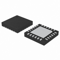
C8051F902-GM Silicon Laboratories Inc, C8051F902-GM Datasheet - Page 225

C8051F902-GM
Manufacturer Part Number
C8051F902-GM
Description
IC MCU 8BIT 8KB FLASH 24QFN
Manufacturer
Silicon Laboratories Inc
Series
C8051F9xxr
Specifications of C8051F902-GM
Program Memory Type
FLASH
Program Memory Size
8KB (8K x 8)
Package / Case
24-QFN
Core Processor
8051
Core Size
8-Bit
Speed
25MHz
Connectivity
SMBus (2-Wire/I²C), SPI, UART/USART
Peripherals
Brown-out Detect/Reset, POR, PWM, Temp Sensor, WDT
Number Of I /o
16
Ram Size
768 x 8
Voltage - Supply (vcc/vdd)
0.9 V ~ 3.6 V
Data Converters
A/D 15x10/12b
Oscillator Type
Internal
Operating Temperature
-40°C ~ 85°C
Processor Series
C8051F9x
Core
8051
Data Ram Size
768 B
Interface Type
UART
Maximum Clock Frequency
25 MHz
Number Of Timers
4
Operating Supply Voltage
0.9 V to 3.6 V
Maximum Operating Temperature
+ 85 C
Mounting Style
SMD/SMT
3rd Party Development Tools
PK51, CA51, A51, ULINK2
Development Tools By Supplier
C8051F912DK
Minimum Operating Temperature
- 40 C
On-chip Adc
12 bit
Package
24QFN EP
Device Core
8051
Family Name
C8051F90x
Maximum Speed
25 MHz
Data Bus Width
8 Bit
Number Of Programmable I/os
16
Lead Free Status / RoHS Status
Lead free / RoHS Compliant
Eeprom Size
-
Lead Free Status / Rohs Status
Lead free / RoHS Compliant
Other names
336-1848-5
- Current page: 225 of 318
- Download datasheet (3Mb)
22. SMBus
The SMBus I/O interface is a two-wire, bi-directional serial bus. The SMBus is compliant with the System
Management Bus Specification, version 1.1, and compatible with the I
the interface by the system controller are byte oriented with the SMBus interface autonomously controlling
the serial transfer of the data. Data can be transferred at up to 1/20th of the system clock as a master or
slave (this can be faster than allowed by the SMBus specification, depending on the system clock used). A
method of extending the clock-low duration is available to accommodate devices with different speed
capabilities on the same bus.
The SMBus interface may operate as a master and/or slave, and may function on a bus with multiple mas-
ters. The SMBus provides control of SDA (serial data), SCL (serial clock) generation and synchronization,
arbitration logic, and START/STOP control and generation. The SMBus peripheral can be fully driven by
software (i.e. software accepts/rejects slave addresses, and generates ACKs), or hardware slave address
recognition and automatic ACK generation can be enabled to minimize software overhead. A block dia-
gram of the SMBus peripheral and the associated SFRs is shown in Figure 22.1.
S
V
L
6
M
A
S
T
E
R
Interrupt
Request
S
V
L
5
M
O
D
T
X
E
SMB0ADR
S
V
L
4
SMB0CN
S
T
A
S
L
V
3
S
O
T
S
V
L
2
Q
A
C
K
R
S
L
V
1
A
R
B
O
S
L
T
S
V
L
0
C
A
K
G
C
S
I
S
V
M
L
6
Arbitration
SCL Synchronization
SCL Generation (Master Mode)
SDA Control
Hardware Slave Address Recognition
Hardware ACK Generation
IRQ Generation
M
SMBUS CONTROL LOGIC
S
L
V
5
SMB0ADM
M
S
V
L
4
M
S
L
V
3
M
S
V
L
2
M
E
N
S
B
Figure 22.1. SMBus Block Diagram
M
S
L
V
1
N
H
I
M
S
V
L
0
SMB0CF
B
U
S
Y
E
H
A
C
K
E
X
H
O
D
T
L
M
O
S
B
T
E
M
S
B
F
T
E
M
C
S
B
S
1
7
M
S
B
C
S
0
6
Data Path
SMB0DAT
5
Control
4
3
Rev. 1.0
2
1
0
00
01
10
11
Control
SDA
Control
SCL
C8051F91x-C8051F90x
T0 Overflow
T1 Overflow
TMR2H Overflow
TMR2L Overflow
FILTER
FILTER
2
N
N
C serial bus. Reads and writes to
SDA
SCL
C
R
O
S
S
B
A
R
Port I/O
225
Related parts for C8051F902-GM
Image
Part Number
Description
Manufacturer
Datasheet
Request
R
Part Number:
Description:
SMD/C°/SINGLE-ENDED OUTPUT SILICON OSCILLATOR
Manufacturer:
Silicon Laboratories Inc
Part Number:
Description:
Manufacturer:
Silicon Laboratories Inc
Datasheet:
Part Number:
Description:
N/A N/A/SI4010 AES KEYFOB DEMO WITH LCD RX
Manufacturer:
Silicon Laboratories Inc
Datasheet:
Part Number:
Description:
N/A N/A/SI4010 SIMPLIFIED KEY FOB DEMO WITH LED RX
Manufacturer:
Silicon Laboratories Inc
Datasheet:
Part Number:
Description:
N/A/-40 TO 85 OC/EZLINK MODULE; F930/4432 HIGH BAND (REV E/B1)
Manufacturer:
Silicon Laboratories Inc
Part Number:
Description:
EZLink Module; F930/4432 Low Band (rev e/B1)
Manufacturer:
Silicon Laboratories Inc
Part Number:
Description:
I°/4460 10 DBM RADIO TEST CARD 434 MHZ
Manufacturer:
Silicon Laboratories Inc
Part Number:
Description:
I°/4461 14 DBM RADIO TEST CARD 868 MHZ
Manufacturer:
Silicon Laboratories Inc
Part Number:
Description:
I°/4463 20 DBM RFSWITCH RADIO TEST CARD 460 MHZ
Manufacturer:
Silicon Laboratories Inc
Part Number:
Description:
I°/4463 20 DBM RADIO TEST CARD 868 MHZ
Manufacturer:
Silicon Laboratories Inc
Part Number:
Description:
I°/4463 27 DBM RADIO TEST CARD 868 MHZ
Manufacturer:
Silicon Laboratories Inc
Part Number:
Description:
I°/4463 SKYWORKS 30 DBM RADIO TEST CARD 915 MHZ
Manufacturer:
Silicon Laboratories Inc
Part Number:
Description:
N/A N/A/-40 TO 85 OC/4463 RFMD 30 DBM RADIO TEST CARD 915 MHZ
Manufacturer:
Silicon Laboratories Inc
Part Number:
Description:
I°/4463 20 DBM RADIO TEST CARD 169 MHZ
Manufacturer:
Silicon Laboratories Inc


