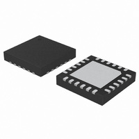
C8051F902-GM Silicon Laboratories Inc, C8051F902-GM Datasheet - Page 189

C8051F902-GM
Manufacturer Part Number
C8051F902-GM
Description
IC MCU 8BIT 8KB FLASH 24QFN
Manufacturer
Silicon Laboratories Inc
Series
C8051F9xxr
Specifications of C8051F902-GM
Program Memory Type
FLASH
Program Memory Size
8KB (8K x 8)
Package / Case
24-QFN
Core Processor
8051
Core Size
8-Bit
Speed
25MHz
Connectivity
SMBus (2-Wire/I²C), SPI, UART/USART
Peripherals
Brown-out Detect/Reset, POR, PWM, Temp Sensor, WDT
Number Of I /o
16
Ram Size
768 x 8
Voltage - Supply (vcc/vdd)
0.9 V ~ 3.6 V
Data Converters
A/D 15x10/12b
Oscillator Type
Internal
Operating Temperature
-40°C ~ 85°C
Processor Series
C8051F9x
Core
8051
Data Ram Size
768 B
Interface Type
UART
Maximum Clock Frequency
25 MHz
Number Of Timers
4
Operating Supply Voltage
0.9 V to 3.6 V
Maximum Operating Temperature
+ 85 C
Mounting Style
SMD/SMT
3rd Party Development Tools
PK51, CA51, A51, ULINK2
Development Tools By Supplier
C8051F912DK
Minimum Operating Temperature
- 40 C
On-chip Adc
12 bit
Package
24QFN EP
Device Core
8051
Family Name
C8051F90x
Maximum Speed
25 MHz
Data Bus Width
8 Bit
Number Of Programmable I/os
16
Lead Free Status / RoHS Status
Lead free / RoHS Compliant
Eeprom Size
-
Lead Free Status / Rohs Status
Lead free / RoHS Compliant
Other names
336-1848-5
- Current page: 189 of 318
- Download datasheet (3Mb)
20.1. SmaRTClock Interface
The SmaRTClock Interface consists of three registers: RTC0KEY, RTC0ADR, and RTC0DAT. These
interface registers are located on the CIP-51’s SFR map and provide access to the SmaRTClock internal
registers listed in Table 20.1. The SmaRTClock internal registers can only be accessed indirectly through
the SmaRTClock Interface.
Table 20.1. SmaRTClock Internal Registers
20.1.1. SmaRTClock Lock and Key Functions
The SmaRTClock Interface is protected with a lock and key function. The SmaRTClock Lock and Key
Register (RTC0KEY) must be written with the correct key codes, in sequence, before writes and reads to
RTC0ADR and RTC0DAT may be performed. The key codes are: 0xA5, 0xF1. There are no timing
restrictions, but the key codes must be written in order. If the key codes are written out of order, the wrong
codes are written, or an indirect register read or write is attempted while the interface is locked, the
SmaRTClock interface will be disabled, and the RTC0ADR and RTC0DAT registers will become
inaccessible until the next system reset. Once the SmaRTClock interface is unlocked, software may
perform any number of accesses to the SmaRTClock registers until the interface is re-locked or the device
is reset. Any write to RTC0KEY while the SmaRTClock interface is unlocked will re-lock the interface.
Reading the RTC0KEY register at any time will provide the SmaRTClock Interface status and will not
interfere with the sequence that is being written. The RTC0KEY register description in SFR Definition 20.1
lists the definition of each status code.
SmaRTClock
0x08–0x0B
0x00–0x03
Address
0x04
0x05
0x06
0x07
SmaRTClock
CAPTUREn SmaRTClock Capture
RTC0XCN
RTC0XCF
RTC0PIN
Register
RTC0CN
ALARMn
Registers
SmaRTClock Control
Register
SmaRTClock Oscillator
Control Register
SmaRTClock Oscillator
Configuration Register
SmaRTClock Pin
Configuration Register
SmaRTClock Alarm
Registers
Register Name
Rev. 1.0
C8051F91x-C8051F90x
Four Registers used for setting the 32-bit
SmaRTClock timer or reading its current value.
Controls the operation of the SmaRTClock State
Machine.
Controls the operation of the SmaRTClock
Oscillator.
Note: Some bits in this register are only available on
Controls the value of the progammable
oscillator load capacitance and
enables/disables AutoStep.
Forces XTAL3 and XTAL4 to be internally
shorted.
Note: This register also contains other reserved bits
Four registers used for setting or reading the
32-bit SmaRTClock alarm value.
‘F912 and ‘F902 devices.
which should not be modified.
Description
189
Related parts for C8051F902-GM
Image
Part Number
Description
Manufacturer
Datasheet
Request
R
Part Number:
Description:
SMD/C°/SINGLE-ENDED OUTPUT SILICON OSCILLATOR
Manufacturer:
Silicon Laboratories Inc
Part Number:
Description:
Manufacturer:
Silicon Laboratories Inc
Datasheet:
Part Number:
Description:
N/A N/A/SI4010 AES KEYFOB DEMO WITH LCD RX
Manufacturer:
Silicon Laboratories Inc
Datasheet:
Part Number:
Description:
N/A N/A/SI4010 SIMPLIFIED KEY FOB DEMO WITH LED RX
Manufacturer:
Silicon Laboratories Inc
Datasheet:
Part Number:
Description:
N/A/-40 TO 85 OC/EZLINK MODULE; F930/4432 HIGH BAND (REV E/B1)
Manufacturer:
Silicon Laboratories Inc
Part Number:
Description:
EZLink Module; F930/4432 Low Band (rev e/B1)
Manufacturer:
Silicon Laboratories Inc
Part Number:
Description:
I°/4460 10 DBM RADIO TEST CARD 434 MHZ
Manufacturer:
Silicon Laboratories Inc
Part Number:
Description:
I°/4461 14 DBM RADIO TEST CARD 868 MHZ
Manufacturer:
Silicon Laboratories Inc
Part Number:
Description:
I°/4463 20 DBM RFSWITCH RADIO TEST CARD 460 MHZ
Manufacturer:
Silicon Laboratories Inc
Part Number:
Description:
I°/4463 20 DBM RADIO TEST CARD 868 MHZ
Manufacturer:
Silicon Laboratories Inc
Part Number:
Description:
I°/4463 27 DBM RADIO TEST CARD 868 MHZ
Manufacturer:
Silicon Laboratories Inc
Part Number:
Description:
I°/4463 SKYWORKS 30 DBM RADIO TEST CARD 915 MHZ
Manufacturer:
Silicon Laboratories Inc
Part Number:
Description:
N/A N/A/-40 TO 85 OC/4463 RFMD 30 DBM RADIO TEST CARD 915 MHZ
Manufacturer:
Silicon Laboratories Inc
Part Number:
Description:
I°/4463 20 DBM RADIO TEST CARD 169 MHZ
Manufacturer:
Silicon Laboratories Inc


