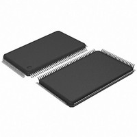
AT91SAM7L64-AU Atmel, AT91SAM7L64-AU Datasheet - Page 552

AT91SAM7L64-AU
Manufacturer Part Number
AT91SAM7L64-AU
Description
MCU ARM7 64K HS FLASH 128-LQFP
Manufacturer
Atmel
Series
AT91SAMr
Specifications of AT91SAM7L64-AU
Core Processor
ARM7
Core Size
16/32-Bit
Speed
36MHz
Connectivity
I²C, SPI, UART/USART
Peripherals
Brown-out Detect/Reset, LCD, POR, PWM, WDT
Number Of I /o
80
Program Memory Size
64KB (64K x 8)
Program Memory Type
FLASH
Ram Size
6K x 8
Voltage - Supply (vcc/vdd)
1.55 V ~ 1.8 V
Data Converters
A/D 4x10b
Oscillator Type
Internal
Operating Temperature
-40°C ~ 85°C
Package / Case
128-LQFP
Controller Family/series
AT91SAM7xxx
No. Of I/o's
80
Ram Memory Size
6KB
Cpu Speed
36MHz
No. Of Timers
1
Rohs Compliant
Yes
Processor Series
AT91SAMx
Core
ARM7TDMI
Data Bus Width
32 bit
Data Ram Size
6 KB
Interface Type
2-Wire, SPI, USART
Maximum Clock Frequency
36 MHz
Number Of Programmable I/os
80
Number Of Timers
3
Maximum Operating Temperature
+ 85 C
Mounting Style
SMD/SMT
3rd Party Development Tools
JTRACE-ARM-2M, MDK-ARM, RL-ARM, ULINK2
Development Tools By Supplier
AT91SAM-ICE, AT91-ISP, AT91SAM7L-EK
Minimum Operating Temperature
- 40 C
On-chip Adc
10 bit, 4 Channel
For Use With
AT91SAM7L-STK - KIT EVAL FOR AT91SAM7LAT91SAM-ICE - EMULATOR FOR AT91 ARM7/ARM9
Lead Free Status / RoHS Status
Lead free / RoHS Compliant
Eeprom Size
-
Lead Free Status / Rohs Status
Details
Available stocks
Company
Part Number
Manufacturer
Quantity
Price
- Current page: 552 of 564
- Download datasheet (9Mb)
38.2
38.2.1
38.2.1.1
38.2.2
38.2.2.1
38.2.3
38.2.3.1
38.2.3.2
552
AT91SAM7L128/64
AT91SAM7L128/64 Preliminary
Analog-to-Digital Converter (ADC)
Pulse Width Modulation Controller (PWM)
Serial Peripheral Interface (SPI)
ADC: Sleep Mode
PWM: Counter Start Value
SPI: Baudrate Set to 1
SPI: Bad Serial Clock Generation on 2nd Chip Select
Refer to
If Sleep mode is activated while there is no activity (no conversion is being performed), it will
take effect only after a conversion occurs.
To activate sleep mode as soon as possible, it is recommended to write successively, ADC
Mode Register (SLEEP) then ADC Control Register (START bit field), in order to start an analog-
todigital conversion and then put ADC into sleep mode at the end of this conversion.
In left aligned mode, the first start value of the counter is 0. For the other periods, the counter
starts at 1.
None.
When the Baudrate is set at 1 (so, the serial clock frequency equals the master clock), and when
the BITS field (number of bits to be transmitted) in SPI_CSRx equals an odd value (in this case
9, 11, 13 or 15), an additional pulse will be generated on SPCK.
It does not occur when the BITS field is equal to 8, 10, 12, 14 or 16 and the Baudrate is equal
to 1.
None.
Bad Serial clock generation on the 2nd chip select when SCBR = 1, CPOL = 1 and NCPHA = 0.
This occurs using SPI with the following conditions:
Do not use a multiple Chip Select configuration where at least one SCRx register is configured
with SCBR = 1 and the others differ from 1 if NCPHA = 0 and CPOL = 1.
• Master Mode
• CPOL = 1 and NCPHA = 0
• Multiple chip selects are used with one transfer with Baud rate (SCBR) equal to 1 (i.e., when
• Transmitting with the slowest chip select and then with the fastest one, then an additional
serial clock frequency equals the system clock frequency) and the other transfers set with
SCBR are not equal to 1
pulse is generated on output SPCK during the second transfer.
Problem Fix/Workaround
Problem Fix/Workaround
Problem Fix/Workaround
Problem Fix/Workaround
Section 38.1 “Marking” on page
551.
6257A–ATARM–20-Feb-08
Related parts for AT91SAM7L64-AU
Image
Part Number
Description
Manufacturer
Datasheet
Request
R

Part Number:
Description:
KIT EVAL FOR AT91SAM7L
Manufacturer:
Atmel
Datasheet:

Part Number:
Description:
DEV KIT FOR AVR/AVR32
Manufacturer:
Atmel
Datasheet:

Part Number:
Description:
INTERVAL AND WIPE/WASH WIPER CONTROL IC WITH DELAY
Manufacturer:
ATMEL Corporation
Datasheet:

Part Number:
Description:
Low-Voltage Voice-Switched IC for Hands-Free Operation
Manufacturer:
ATMEL Corporation
Datasheet:

Part Number:
Description:
MONOLITHIC INTEGRATED FEATUREPHONE CIRCUIT
Manufacturer:
ATMEL Corporation
Datasheet:

Part Number:
Description:
AM-FM Receiver IC U4255BM-M
Manufacturer:
ATMEL Corporation
Datasheet:

Part Number:
Description:
Monolithic Integrated Feature Phone Circuit
Manufacturer:
ATMEL Corporation
Datasheet:

Part Number:
Description:
Multistandard Video-IF and Quasi Parallel Sound Processing
Manufacturer:
ATMEL Corporation
Datasheet:

Part Number:
Description:
High-performance EE PLD
Manufacturer:
ATMEL Corporation
Datasheet:

Part Number:
Description:
8-bit Flash Microcontroller
Manufacturer:
ATMEL Corporation
Datasheet:

Part Number:
Description:
2-Wire Serial EEPROM
Manufacturer:
ATMEL Corporation
Datasheet:


