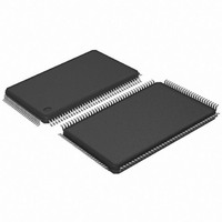
AT91SAM7L64-AU Atmel, AT91SAM7L64-AU Datasheet - Page 12

AT91SAM7L64-AU
Manufacturer Part Number
AT91SAM7L64-AU
Description
MCU ARM7 64K HS FLASH 128-LQFP
Manufacturer
Atmel
Series
AT91SAMr
Specifications of AT91SAM7L64-AU
Core Processor
ARM7
Core Size
16/32-Bit
Speed
36MHz
Connectivity
I²C, SPI, UART/USART
Peripherals
Brown-out Detect/Reset, LCD, POR, PWM, WDT
Number Of I /o
80
Program Memory Size
64KB (64K x 8)
Program Memory Type
FLASH
Ram Size
6K x 8
Voltage - Supply (vcc/vdd)
1.55 V ~ 1.8 V
Data Converters
A/D 4x10b
Oscillator Type
Internal
Operating Temperature
-40°C ~ 85°C
Package / Case
128-LQFP
Controller Family/series
AT91SAM7xxx
No. Of I/o's
80
Ram Memory Size
6KB
Cpu Speed
36MHz
No. Of Timers
1
Rohs Compliant
Yes
Processor Series
AT91SAMx
Core
ARM7TDMI
Data Bus Width
32 bit
Data Ram Size
6 KB
Interface Type
2-Wire, SPI, USART
Maximum Clock Frequency
36 MHz
Number Of Programmable I/os
80
Number Of Timers
3
Maximum Operating Temperature
+ 85 C
Mounting Style
SMD/SMT
3rd Party Development Tools
JTRACE-ARM-2M, MDK-ARM, RL-ARM, ULINK2
Development Tools By Supplier
AT91SAM-ICE, AT91-ISP, AT91SAM7L-EK
Minimum Operating Temperature
- 40 C
On-chip Adc
10 bit, 4 Channel
For Use With
AT91SAM7L-STK - KIT EVAL FOR AT91SAM7LAT91SAM-ICE - EMULATOR FOR AT91 ARM7/ARM9
Lead Free Status / RoHS Status
Lead free / RoHS Compliant
Eeprom Size
-
Lead Free Status / Rohs Status
Details
Available stocks
Company
Part Number
Manufacturer
Quantity
Price
- Current page: 12 of 564
- Download datasheet (9Mb)
5. Power Considerations
5.1
5.2
5.2.1
5.2.2
12
Power Supplies
Low Power Modes
AT91SAM7L128/64 Preliminary
Off (Power Down) Mode
Backup Mode
The AT91SAM7L128/64 has six types of power supply pins and integrates a voltage regulator,
allowing the device to be supplied with only one voltage. The six power supply pin types are:
No separate ground pins are provided for the different power supplies. Only GND pins are pro-
vided and should be connected as shortly as possible to the system ground plane.
The various low power modes of the AT91SAM7L128/64 are described below.
In off (power down) mode, the entire chip is shut down. Only a low level on the FWUP pin can
wake up the AT91SAM7L128/64 (by a push-button for example). Internally, except for the
FWUP pin through VDDIO1, none of the chip is supplied.
Once the internal main power switch has been activated by FWUP, the 32 kHz RC oscillator and
the Supply Controller are supplied, then the core and peripherals are reset and the
AT91SAM7L128/64 enters in active mode. Refer to the System Controller Block Diagram,
ure 9-1 on page
At first power-up, if FWUP is tied high, the device enters off mode. The PIOA and PIOB pins’
states are undefined. PIOC and NRST pins are initialized as high impedance inputs.
Once the device enters active mode, the core and the parallel input/output controller are reset.
Then, if the chip enters off mode, PIOA and PIOB pins are configured as inputs with pull-ups and
PIOC pins as high impedance inputs.
Current consumption in this mode is typically 100 nA.
In backup mode, the supply controller, the zero-power power-on reset and the 32 kHz oscillator
(software selectable internal RC or external crystal) remain running. The voltage regulator and
the core are switched off.
Prior to entering this mode, the RTC, the backup SRAM, the brownout detector, the charge
pump, the LCD voltage regulator and the LCD controller can be set on or off separately.
• VDDOUT pin. It is the output of the voltage regulator. Output voltage can be programmed
• VDDIO1 pin. It powers the voltage regulator input and all the PIOC IO lines (1.8V-3.6V).
• VDDIO2 pin. It powers the PIOA and PIOB I/O lines (1.8V-3.6V). It is also the output of the
• VDDCORE pin. It powers the logic of the device, the PLL, the 2 MHz Fast RC oscillator, the
• VDDINLCD pin. It powers the charge pump which can be used as LCD Regulator power
from 1.55V to 1.80V by steps of 100 mV.
VDDIO1 voltage must be above 2.2V to allow the chip to start-up (POR threshold).
LCD voltage regulator. The output voltage can be programmed from 2.4V to 3.4V with 16
steps.
ADC and the Flash memory. It must be connected to the VDDOUT pin with a decoupling
capacitor.
supply. Voltage ranges from 1.8V to 3.6V.
30.
6257A–ATARM–20-Feb-08
Fig-
Related parts for AT91SAM7L64-AU
Image
Part Number
Description
Manufacturer
Datasheet
Request
R

Part Number:
Description:
KIT EVAL FOR AT91SAM7L
Manufacturer:
Atmel
Datasheet:

Part Number:
Description:
DEV KIT FOR AVR/AVR32
Manufacturer:
Atmel
Datasheet:

Part Number:
Description:
INTERVAL AND WIPE/WASH WIPER CONTROL IC WITH DELAY
Manufacturer:
ATMEL Corporation
Datasheet:

Part Number:
Description:
Low-Voltage Voice-Switched IC for Hands-Free Operation
Manufacturer:
ATMEL Corporation
Datasheet:

Part Number:
Description:
MONOLITHIC INTEGRATED FEATUREPHONE CIRCUIT
Manufacturer:
ATMEL Corporation
Datasheet:

Part Number:
Description:
AM-FM Receiver IC U4255BM-M
Manufacturer:
ATMEL Corporation
Datasheet:

Part Number:
Description:
Monolithic Integrated Feature Phone Circuit
Manufacturer:
ATMEL Corporation
Datasheet:

Part Number:
Description:
Multistandard Video-IF and Quasi Parallel Sound Processing
Manufacturer:
ATMEL Corporation
Datasheet:

Part Number:
Description:
High-performance EE PLD
Manufacturer:
ATMEL Corporation
Datasheet:

Part Number:
Description:
8-bit Flash Microcontroller
Manufacturer:
ATMEL Corporation
Datasheet:

Part Number:
Description:
2-Wire Serial EEPROM
Manufacturer:
ATMEL Corporation
Datasheet:


