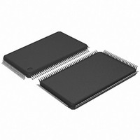
AT91SAM7L64-AU Atmel, AT91SAM7L64-AU Datasheet - Page 216

AT91SAM7L64-AU
Manufacturer Part Number
AT91SAM7L64-AU
Description
MCU ARM7 64K HS FLASH 128-LQFP
Manufacturer
Atmel
Series
AT91SAMr
Specifications of AT91SAM7L64-AU
Core Processor
ARM7
Core Size
16/32-Bit
Speed
36MHz
Connectivity
I²C, SPI, UART/USART
Peripherals
Brown-out Detect/Reset, LCD, POR, PWM, WDT
Number Of I /o
80
Program Memory Size
64KB (64K x 8)
Program Memory Type
FLASH
Ram Size
6K x 8
Voltage - Supply (vcc/vdd)
1.55 V ~ 1.8 V
Data Converters
A/D 4x10b
Oscillator Type
Internal
Operating Temperature
-40°C ~ 85°C
Package / Case
128-LQFP
Controller Family/series
AT91SAM7xxx
No. Of I/o's
80
Ram Memory Size
6KB
Cpu Speed
36MHz
No. Of Timers
1
Rohs Compliant
Yes
Processor Series
AT91SAMx
Core
ARM7TDMI
Data Bus Width
32 bit
Data Ram Size
6 KB
Interface Type
2-Wire, SPI, USART
Maximum Clock Frequency
36 MHz
Number Of Programmable I/os
80
Number Of Timers
3
Maximum Operating Temperature
+ 85 C
Mounting Style
SMD/SMT
3rd Party Development Tools
JTRACE-ARM-2M, MDK-ARM, RL-ARM, ULINK2
Development Tools By Supplier
AT91SAM-ICE, AT91-ISP, AT91SAM7L-EK
Minimum Operating Temperature
- 40 C
On-chip Adc
10 bit, 4 Channel
For Use With
AT91SAM7L-STK - KIT EVAL FOR AT91SAM7LAT91SAM-ICE - EMULATOR FOR AT91 ARM7/ARM9
Lead Free Status / RoHS Status
Lead free / RoHS Compliant
Eeprom Size
-
Lead Free Status / Rohs Status
Details
Available stocks
Company
Part Number
Manufacturer
Quantity
Price
- Current page: 216 of 564
- Download datasheet (9Mb)
24.5.2
24.5.3
24.6
24.6.1
216
Divider and PLL Block
AT91SAM7L128/64 Preliminary
Main Clock Frequency Counter
External Clock CLKIN
PLL Filter
The device features a Main Clock frequency counter that provides the frequency of the Main
Clock.
The Main Clock frequency counter starts incrementing at the Main Clock speed after the next ris-
ing edge of the Slow Clock as soon as MAINCKON is set to 1.Then, at the 16th falling edge of
Slow Clock, the MAINFRDY bit in the Clock Generator Main Clock Frequency Register
(CKGR_MCFR) is set and the counter stops counting. Its value can be read in the MAINF field of
CKGR_MCFR and gives the number of Main Clock cycles during 16 periods of Slow Clock, so
that the frequency of the 2 MHz Fast RC Oscillator or CLKIN input signal can be determined.
The user can input a clock on the device. In this case, the user has to provide the external clock
signal on the CLKIN pin. The programmer has to be sure to set the MCKSEL bit in the Clock
Generator Main Oscillator Register (CKGR_MOR) to 1 for the external clock to operate properly.
The user can check the MAINSELS bit in the Power Management Status Register (PMC_SR) to
check that the selection has been completed.
Note that the user must be sure to put MCKSEL bit to 1 only when an external clock is applied
on CLKIN. The user does not need to check MAINRDY bit when switching to CLKIN.
Input characteristics of the CLKIN pin are given in the Electrical Characteristics section.
The PLL embeds an input divider to increase the accuracy of the resulting clock signals. How-
ever, the user must respect the PLL minimum input frequency when programming the divider.
Figure 24-4
Figure 24-4. Divider and PLL Block Diagram
The PLL requires connection to an external second-order filter through the PLLRC pin.
24-5
shows a schematic of these filters.
shows the block diagram of the divider and PLL block.
SLCK
SLCK
Divider = 1
DIV
PLLCOUNT
Counter
PLLRC
PLL
MUL
PLL
OUT
LOCK
PLLCK
6257A–ATARM–20-Feb-08
Figure
Related parts for AT91SAM7L64-AU
Image
Part Number
Description
Manufacturer
Datasheet
Request
R

Part Number:
Description:
KIT EVAL FOR AT91SAM7L
Manufacturer:
Atmel
Datasheet:

Part Number:
Description:
DEV KIT FOR AVR/AVR32
Manufacturer:
Atmel
Datasheet:

Part Number:
Description:
INTERVAL AND WIPE/WASH WIPER CONTROL IC WITH DELAY
Manufacturer:
ATMEL Corporation
Datasheet:

Part Number:
Description:
Low-Voltage Voice-Switched IC for Hands-Free Operation
Manufacturer:
ATMEL Corporation
Datasheet:

Part Number:
Description:
MONOLITHIC INTEGRATED FEATUREPHONE CIRCUIT
Manufacturer:
ATMEL Corporation
Datasheet:

Part Number:
Description:
AM-FM Receiver IC U4255BM-M
Manufacturer:
ATMEL Corporation
Datasheet:

Part Number:
Description:
Monolithic Integrated Feature Phone Circuit
Manufacturer:
ATMEL Corporation
Datasheet:

Part Number:
Description:
Multistandard Video-IF and Quasi Parallel Sound Processing
Manufacturer:
ATMEL Corporation
Datasheet:

Part Number:
Description:
High-performance EE PLD
Manufacturer:
ATMEL Corporation
Datasheet:

Part Number:
Description:
8-bit Flash Microcontroller
Manufacturer:
ATMEL Corporation
Datasheet:

Part Number:
Description:
2-Wire Serial EEPROM
Manufacturer:
ATMEL Corporation
Datasheet:


