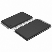
AT91SAM7L64-AU Atmel, AT91SAM7L64-AU Datasheet - Page 160

AT91SAM7L64-AU
Manufacturer Part Number
AT91SAM7L64-AU
Description
MCU ARM7 64K HS FLASH 128-LQFP
Manufacturer
Atmel
Series
AT91SAMr
Specifications of AT91SAM7L64-AU
Core Processor
ARM7
Core Size
16/32-Bit
Speed
36MHz
Connectivity
I²C, SPI, UART/USART
Peripherals
Brown-out Detect/Reset, LCD, POR, PWM, WDT
Number Of I /o
80
Program Memory Size
64KB (64K x 8)
Program Memory Type
FLASH
Ram Size
6K x 8
Voltage - Supply (vcc/vdd)
1.55 V ~ 1.8 V
Data Converters
A/D 4x10b
Oscillator Type
Internal
Operating Temperature
-40°C ~ 85°C
Package / Case
128-LQFP
Controller Family/series
AT91SAM7xxx
No. Of I/o's
80
Ram Memory Size
6KB
Cpu Speed
36MHz
No. Of Timers
1
Rohs Compliant
Yes
Processor Series
AT91SAMx
Core
ARM7TDMI
Data Bus Width
32 bit
Data Ram Size
6 KB
Interface Type
2-Wire, SPI, USART
Maximum Clock Frequency
36 MHz
Number Of Programmable I/os
80
Number Of Timers
3
Maximum Operating Temperature
+ 85 C
Mounting Style
SMD/SMT
3rd Party Development Tools
JTRACE-ARM-2M, MDK-ARM, RL-ARM, ULINK2
Development Tools By Supplier
AT91SAM-ICE, AT91-ISP, AT91SAM7L-EK
Minimum Operating Temperature
- 40 C
On-chip Adc
10 bit, 4 Channel
For Use With
AT91SAM7L-STK - KIT EVAL FOR AT91SAM7LAT91SAM-ICE - EMULATOR FOR AT91 ARM7/ARM9
Lead Free Status / RoHS Status
Lead free / RoHS Compliant
Eeprom Size
-
Lead Free Status / Rohs Status
Details
Available stocks
Company
Part Number
Manufacturer
Quantity
Price
- Current page: 160 of 564
- Download datasheet (9Mb)
20.2.3
20.2.4
20.2.4.1
160
AT91SAM7L128/64 Preliminary
Entering Programming Mode
Programmer Handshaking
Write Handshaking
Table 20-3.
The following algorithm puts the device in Parallel Programming Mode:
A handshake is defined for read and write operations. When the device is ready to start a new
operation (RDY signal set), the programmer starts the handshake by clearing the NCMD signal.
The handshaking is achieved once NCMD signal is high and RDY is high.
For details on the write handshaking sequence, refer to
Figure 20-3. Parallel Programming Timing, Write Sequence
DATA[15:0]
0x0044
0x0025
0x0054
0x0035
0x001F
0x001E
• Apply GND, TST, CLKIN, FWUP and the supplies as described in table 4.1.
• Apply XIN clock
• Wait for 20 ms
• Start a read or write handshaking.
MODE[3:0]
DATA[15:0]
NVALID
Command Bit Coding (Continued)
NCMD
NOE
RDY
1
Symbol
CGPB
GGPB
SSE
GSE
WRAM
GVE
2
3
Command Executed
Clear General Purpose NVM bit
Get General Purpose NVM bit
Set Security Bit
Get Security Bit
Write Memory
Get Version
Figure 20-3
4
5
and
Table
6257A–ATARM–20-Feb-08
20-4.
Related parts for AT91SAM7L64-AU
Image
Part Number
Description
Manufacturer
Datasheet
Request
R

Part Number:
Description:
KIT EVAL FOR AT91SAM7L
Manufacturer:
Atmel
Datasheet:

Part Number:
Description:
DEV KIT FOR AVR/AVR32
Manufacturer:
Atmel
Datasheet:

Part Number:
Description:
INTERVAL AND WIPE/WASH WIPER CONTROL IC WITH DELAY
Manufacturer:
ATMEL Corporation
Datasheet:

Part Number:
Description:
Low-Voltage Voice-Switched IC for Hands-Free Operation
Manufacturer:
ATMEL Corporation
Datasheet:

Part Number:
Description:
MONOLITHIC INTEGRATED FEATUREPHONE CIRCUIT
Manufacturer:
ATMEL Corporation
Datasheet:

Part Number:
Description:
AM-FM Receiver IC U4255BM-M
Manufacturer:
ATMEL Corporation
Datasheet:

Part Number:
Description:
Monolithic Integrated Feature Phone Circuit
Manufacturer:
ATMEL Corporation
Datasheet:

Part Number:
Description:
Multistandard Video-IF and Quasi Parallel Sound Processing
Manufacturer:
ATMEL Corporation
Datasheet:

Part Number:
Description:
High-performance EE PLD
Manufacturer:
ATMEL Corporation
Datasheet:

Part Number:
Description:
8-bit Flash Microcontroller
Manufacturer:
ATMEL Corporation
Datasheet:

Part Number:
Description:
2-Wire Serial EEPROM
Manufacturer:
ATMEL Corporation
Datasheet:


