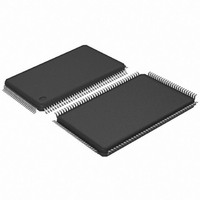
AT91SAM7L64-AU Atmel, AT91SAM7L64-AU Datasheet - Page 115

AT91SAM7L64-AU
Manufacturer Part Number
AT91SAM7L64-AU
Description
MCU ARM7 64K HS FLASH 128-LQFP
Manufacturer
Atmel
Series
AT91SAMr
Specifications of AT91SAM7L64-AU
Core Processor
ARM7
Core Size
16/32-Bit
Speed
36MHz
Connectivity
I²C, SPI, UART/USART
Peripherals
Brown-out Detect/Reset, LCD, POR, PWM, WDT
Number Of I /o
80
Program Memory Size
64KB (64K x 8)
Program Memory Type
FLASH
Ram Size
6K x 8
Voltage - Supply (vcc/vdd)
1.55 V ~ 1.8 V
Data Converters
A/D 4x10b
Oscillator Type
Internal
Operating Temperature
-40°C ~ 85°C
Package / Case
128-LQFP
Controller Family/series
AT91SAM7xxx
No. Of I/o's
80
Ram Memory Size
6KB
Cpu Speed
36MHz
No. Of Timers
1
Rohs Compliant
Yes
Processor Series
AT91SAMx
Core
ARM7TDMI
Data Bus Width
32 bit
Data Ram Size
6 KB
Interface Type
2-Wire, SPI, USART
Maximum Clock Frequency
36 MHz
Number Of Programmable I/os
80
Number Of Timers
3
Maximum Operating Temperature
+ 85 C
Mounting Style
SMD/SMT
3rd Party Development Tools
JTRACE-ARM-2M, MDK-ARM, RL-ARM, ULINK2
Development Tools By Supplier
AT91SAM-ICE, AT91-ISP, AT91SAM7L-EK
Minimum Operating Temperature
- 40 C
On-chip Adc
10 bit, 4 Channel
For Use With
AT91SAM7L-STK - KIT EVAL FOR AT91SAM7LAT91SAM-ICE - EMULATOR FOR AT91 ARM7/ARM9
Lead Free Status / RoHS Status
Lead free / RoHS Compliant
Eeprom Size
-
Lead Free Status / Rohs Status
Details
Available stocks
Company
Part Number
Manufacturer
Quantity
Price
- Current page: 115 of 564
- Download datasheet (9Mb)
17.3.7
6257A–ATARM–20-Feb-08
Wake Up Sources
The Flash Memory is automatically switched on when the core power supply is enabled at start
up.
The status of the Flash Memory, i.e., ready to use, or not ready, can be seen through the
FLASHS field in the status register SUPC_ SR.
There are several restrictions concerning the write of the FLASHON field:
The wake up events allow the device to exit backup mode. When a wake up event is detected,
the Supply Controller performs a sequence which automatically reenables the core power sup-
ply, and the SRAM power supply, if it is not already enabled.
• If FLASHON is written to 1 while it is at 0, after one main clock cycle, the Flash Memory
• If FLASHON is written to 0 while it is at 1, after one main clock cycle, the flag FLASHS is
• The user must check that the previous power supply switch operation is done before writing
• Writing FLASHON at 1 while it is already at 1 or writing FLASHON at 0 while it is already at 0
power switch is closed by resetting the flash_off signal at 0, then after ninety main clock
cycles the FLASHS flag signal is set at 1. This ensures that the Flash Memory is always
properly cleared when its power rises.
reset to 0, then two main clock cycles after, the Flash Memory power switch is opened by
setting the signal, flash_off at 1.
FLASHON again. To do that, the user must check that the FLASHS flag has the correct
value. If FLASHON is written to 0, the FLASHS flag is reset at 0. If FLASHON is written to 1,
the FLASHS flag is set at 1.
is forbidden and has no effect.
AT91SAM7L128/64 Preliminary
115
Related parts for AT91SAM7L64-AU
Image
Part Number
Description
Manufacturer
Datasheet
Request
R

Part Number:
Description:
KIT EVAL FOR AT91SAM7L
Manufacturer:
Atmel
Datasheet:

Part Number:
Description:
DEV KIT FOR AVR/AVR32
Manufacturer:
Atmel
Datasheet:

Part Number:
Description:
INTERVAL AND WIPE/WASH WIPER CONTROL IC WITH DELAY
Manufacturer:
ATMEL Corporation
Datasheet:

Part Number:
Description:
Low-Voltage Voice-Switched IC for Hands-Free Operation
Manufacturer:
ATMEL Corporation
Datasheet:

Part Number:
Description:
MONOLITHIC INTEGRATED FEATUREPHONE CIRCUIT
Manufacturer:
ATMEL Corporation
Datasheet:

Part Number:
Description:
AM-FM Receiver IC U4255BM-M
Manufacturer:
ATMEL Corporation
Datasheet:

Part Number:
Description:
Monolithic Integrated Feature Phone Circuit
Manufacturer:
ATMEL Corporation
Datasheet:

Part Number:
Description:
Multistandard Video-IF and Quasi Parallel Sound Processing
Manufacturer:
ATMEL Corporation
Datasheet:

Part Number:
Description:
High-performance EE PLD
Manufacturer:
ATMEL Corporation
Datasheet:

Part Number:
Description:
8-bit Flash Microcontroller
Manufacturer:
ATMEL Corporation
Datasheet:

Part Number:
Description:
2-Wire Serial EEPROM
Manufacturer:
ATMEL Corporation
Datasheet:


