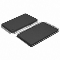
AT91SAM7L64-AU Atmel, AT91SAM7L64-AU Datasheet - Page 502

AT91SAM7L64-AU
Manufacturer Part Number
AT91SAM7L64-AU
Description
MCU ARM7 64K HS FLASH 128-LQFP
Manufacturer
Atmel
Series
AT91SAMr
Specifications of AT91SAM7L64-AU
Core Processor
ARM7
Core Size
16/32-Bit
Speed
36MHz
Connectivity
I²C, SPI, UART/USART
Peripherals
Brown-out Detect/Reset, LCD, POR, PWM, WDT
Number Of I /o
80
Program Memory Size
64KB (64K x 8)
Program Memory Type
FLASH
Ram Size
6K x 8
Voltage - Supply (vcc/vdd)
1.55 V ~ 1.8 V
Data Converters
A/D 4x10b
Oscillator Type
Internal
Operating Temperature
-40°C ~ 85°C
Package / Case
128-LQFP
Controller Family/series
AT91SAM7xxx
No. Of I/o's
80
Ram Memory Size
6KB
Cpu Speed
36MHz
No. Of Timers
1
Rohs Compliant
Yes
Processor Series
AT91SAMx
Core
ARM7TDMI
Data Bus Width
32 bit
Data Ram Size
6 KB
Interface Type
2-Wire, SPI, USART
Maximum Clock Frequency
36 MHz
Number Of Programmable I/os
80
Number Of Timers
3
Maximum Operating Temperature
+ 85 C
Mounting Style
SMD/SMT
3rd Party Development Tools
JTRACE-ARM-2M, MDK-ARM, RL-ARM, ULINK2
Development Tools By Supplier
AT91SAM-ICE, AT91-ISP, AT91SAM7L-EK
Minimum Operating Temperature
- 40 C
On-chip Adc
10 bit, 4 Channel
For Use With
AT91SAM7L-STK - KIT EVAL FOR AT91SAM7LAT91SAM-ICE - EMULATOR FOR AT91 ARM7/ARM9
Lead Free Status / RoHS Status
Lead free / RoHS Compliant
Eeprom Size
-
Lead Free Status / Rohs Status
Details
Available stocks
Company
Part Number
Manufacturer
Quantity
Price
- Current page: 502 of 564
- Download datasheet (9Mb)
34.5.6
34.5.7
34.5.7.1
502
AT91SAM7L128/64 Preliminary
Buffer Swap Mode
Disable Sequence
Disable Bit
This mode allows to assign all pixels to two states alternatively without reloading the user buffer
at each change.
The means to alternatively display two states is as follows:
Now, each state is alternatively displayed at LCDBLKFREQ frequency.
Except for the phase dealing with the storage of the two display states, the management of the
Buffer Swap Mode is the same as the standard blinking mode.
There are two ways to disable the SLCDC:
In both cases, no DC voltage should be left across any segment.
When the LCD Disable Command is activated during a frame, the next frame will be generated
in “All Ground” Mode (whereby all commons and segments will be tied to ground).
At the end of this ‘All Ground” frame, the disable bit is reset and the disable interrupt is asserted.
This indicates that the SLCDC is really disabled and that the LCD can be switched off.
1. Initially, the SLCDC must be in normal mode or in a standard blinking mode.
2. Data corresponding to the first pixel state is written in the user buffer (through the
3. Wait two ENDFRAME events (to be sure that the user buffer is entirely transferred in
4. SLCDC_DR must be programmed with DISPMODE = 6 (User Buffer Only Load Mode).
5. Wait ENDFRAME event. (The display mode is internally updated at the beginning of
6. Data corresponding to the second pixel state is written in the user buffer (through the
7. SLCDC_DR must be programmed with DISPMODE = 7 (buffer swap mode) and LCD-
1. By using the disable bit. (In this case, register configuration and SLCDC memory are
2. Or by using the software reset bit that acts like a hardware reset.
SLCDC_MEM registers).
the display buffer).
This mode blocks the automatic transfer from the user buffer to the display buffer.
each frame.)
SLCDC_MEM registers). So, now the first pixel state is in the display buffer and the
second pixel state is in the user buffer.
BLKFREQ must be programmed with the wanted blinking frequency (if not previously
done).
kept.)
6257A–ATARM–20-Feb-08
Related parts for AT91SAM7L64-AU
Image
Part Number
Description
Manufacturer
Datasheet
Request
R

Part Number:
Description:
KIT EVAL FOR AT91SAM7L
Manufacturer:
Atmel
Datasheet:

Part Number:
Description:
DEV KIT FOR AVR/AVR32
Manufacturer:
Atmel
Datasheet:

Part Number:
Description:
INTERVAL AND WIPE/WASH WIPER CONTROL IC WITH DELAY
Manufacturer:
ATMEL Corporation
Datasheet:

Part Number:
Description:
Low-Voltage Voice-Switched IC for Hands-Free Operation
Manufacturer:
ATMEL Corporation
Datasheet:

Part Number:
Description:
MONOLITHIC INTEGRATED FEATUREPHONE CIRCUIT
Manufacturer:
ATMEL Corporation
Datasheet:

Part Number:
Description:
AM-FM Receiver IC U4255BM-M
Manufacturer:
ATMEL Corporation
Datasheet:

Part Number:
Description:
Monolithic Integrated Feature Phone Circuit
Manufacturer:
ATMEL Corporation
Datasheet:

Part Number:
Description:
Multistandard Video-IF and Quasi Parallel Sound Processing
Manufacturer:
ATMEL Corporation
Datasheet:

Part Number:
Description:
High-performance EE PLD
Manufacturer:
ATMEL Corporation
Datasheet:

Part Number:
Description:
8-bit Flash Microcontroller
Manufacturer:
ATMEL Corporation
Datasheet:

Part Number:
Description:
2-Wire Serial EEPROM
Manufacturer:
ATMEL Corporation
Datasheet:


