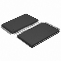
AT91SAM7L64-AU Atmel, AT91SAM7L64-AU Datasheet - Page 168

AT91SAM7L64-AU
Manufacturer Part Number
AT91SAM7L64-AU
Description
MCU ARM7 64K HS FLASH 128-LQFP
Manufacturer
Atmel
Series
AT91SAMr
Specifications of AT91SAM7L64-AU
Core Processor
ARM7
Core Size
16/32-Bit
Speed
36MHz
Connectivity
I²C, SPI, UART/USART
Peripherals
Brown-out Detect/Reset, LCD, POR, PWM, WDT
Number Of I /o
80
Program Memory Size
64KB (64K x 8)
Program Memory Type
FLASH
Ram Size
6K x 8
Voltage - Supply (vcc/vdd)
1.55 V ~ 1.8 V
Data Converters
A/D 4x10b
Oscillator Type
Internal
Operating Temperature
-40°C ~ 85°C
Package / Case
128-LQFP
Controller Family/series
AT91SAM7xxx
No. Of I/o's
80
Ram Memory Size
6KB
Cpu Speed
36MHz
No. Of Timers
1
Rohs Compliant
Yes
Processor Series
AT91SAMx
Core
ARM7TDMI
Data Bus Width
32 bit
Data Ram Size
6 KB
Interface Type
2-Wire, SPI, USART
Maximum Clock Frequency
36 MHz
Number Of Programmable I/os
80
Number Of Timers
3
Maximum Operating Temperature
+ 85 C
Mounting Style
SMD/SMT
3rd Party Development Tools
JTRACE-ARM-2M, MDK-ARM, RL-ARM, ULINK2
Development Tools By Supplier
AT91SAM-ICE, AT91-ISP, AT91SAM7L-EK
Minimum Operating Temperature
- 40 C
On-chip Adc
10 bit, 4 Channel
For Use With
AT91SAM7L-STK - KIT EVAL FOR AT91SAM7LAT91SAM-ICE - EMULATOR FOR AT91 ARM7/ARM9
Lead Free Status / RoHS Status
Lead free / RoHS Compliant
Eeprom Size
-
Lead Free Status / Rohs Status
Details
Available stocks
Company
Part Number
Manufacturer
Quantity
Price
- Current page: 168 of 564
- Download datasheet (9Mb)
20.3.3
168
AT91SAM7L128/64 Preliminary
Read/Write Handshake
Table 20-17. Reset TAP Controller and Go to Select-DR-Scan
The read/write handshake is done by carrying out read/write operations on two registers of the
device that are accessible through the JTAG:
Access to these registers is done through the TAP 38-bit DR register comprising a 32-bit data
field, a 5-bit address field and a read/write bit. The data to be written is scanned into the 32-bit
data field with the address of the register to the 5-bit address field and 1 to the read/write bit. A
register is read by scanning its address into the address field and 0 into the read/write bit, going
through the UPDATE-DR TAP state, then scanning out the data.
Refer to the ARM7TDMI reference manuel for more information on Comm channel operations.
Figure 20-7. TAP 8-bit DR Register
A read or write takes place when the TAP controller enters UPDATE-DR state. Refer to the IEEE
1149.1 for more details on JTAG operations.
• Debug Comms Control Register: DCCR
• Debug Comms Data Register: DCDR
• The address of the Debug Comms Control Register is 0x04.
• The address of the Debug Comms Data Register is 0x05.
TDI
The Debug Comms Control Register is read-only and allows synchronized handshaking
between the processor and the debugger.
– Bit 1 (W): Denotes whether the programmer can read a data through the Debug
Comms Data Register. If the device is busy W = 0, then the programmer must poll
until W = 1.
r/w
TDI
Xt
X
X
X
X
X
X
4
Address
Address
Decoder
5
0
31
TMS
1
1
1
1
1
0
1
TAP Controller State
Test-Logic Reset
Run-Test/Idle
Select-DR-Scan
Debug Comms Control Register
Debug Comms Data Register
Data
32
6257A–ATARM–20-Feb-08
0
TDO
Related parts for AT91SAM7L64-AU
Image
Part Number
Description
Manufacturer
Datasheet
Request
R

Part Number:
Description:
KIT EVAL FOR AT91SAM7L
Manufacturer:
Atmel
Datasheet:

Part Number:
Description:
DEV KIT FOR AVR/AVR32
Manufacturer:
Atmel
Datasheet:

Part Number:
Description:
INTERVAL AND WIPE/WASH WIPER CONTROL IC WITH DELAY
Manufacturer:
ATMEL Corporation
Datasheet:

Part Number:
Description:
Low-Voltage Voice-Switched IC for Hands-Free Operation
Manufacturer:
ATMEL Corporation
Datasheet:

Part Number:
Description:
MONOLITHIC INTEGRATED FEATUREPHONE CIRCUIT
Manufacturer:
ATMEL Corporation
Datasheet:

Part Number:
Description:
AM-FM Receiver IC U4255BM-M
Manufacturer:
ATMEL Corporation
Datasheet:

Part Number:
Description:
Monolithic Integrated Feature Phone Circuit
Manufacturer:
ATMEL Corporation
Datasheet:

Part Number:
Description:
Multistandard Video-IF and Quasi Parallel Sound Processing
Manufacturer:
ATMEL Corporation
Datasheet:

Part Number:
Description:
High-performance EE PLD
Manufacturer:
ATMEL Corporation
Datasheet:

Part Number:
Description:
8-bit Flash Microcontroller
Manufacturer:
ATMEL Corporation
Datasheet:

Part Number:
Description:
2-Wire Serial EEPROM
Manufacturer:
ATMEL Corporation
Datasheet:


