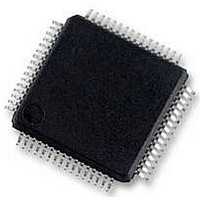
UPD78F0890GK(A)-GAJ-AX NEC, UPD78F0890GK(A)-GAJ-AX Datasheet - Page 730

UPD78F0890GK(A)-GAJ-AX
Manufacturer Part Number
UPD78F0890GK(A)-GAJ-AX
Description
8BIT MCU, 128K FLASH, 7K RAM, LQFP
Manufacturer
NEC
Datasheet
1.UPD78F0890GKA-GAJ-AX.pdf
(732 pages)
Specifications of UPD78F0890GK(A)-GAJ-AX
Controller Family/series
UPD78F
No. Of I/o's
55
Ram Memory Size
7KB
Cpu Speed
20MHz
No. Of Timers
10
No. Of Pwm
RoHS Compliant
Core Size
8bit
Program Memory Size
128KB
Oscillator Type
External, Internal
- Current page: 730 of 732
- Download datasheet (4Mb)
730
3rd
2nd
Edition
• Change of MIN. value of External clock input high level width, low level width, External sub clock input high
• Addition of Peripheral hardware clock frequency and Note 1, 2
• Change of TCY vs. V
• Change of External clock input timing
• Addition of MAX. value of Overall, Conversion time, Zero-scale error, Full-scale error, Integral non-linearity
• Addition of condition
• Addition of MIN. and MAX. value of External input pin
• Addition of Detection voltage on application of supply voltage of Detection voltage
• Change of value of Minimum pulse width
• Change of LVI Circuit Timing
27.4 (1) Basic operation
Change of MAX. value of Transfer rate in (a) UART mode (UART6n, dedicated baud rate generator output)
Change of MIN. value of SCK1n cycle time, SCK1n high-/low-level width, SI1n setup time (to SCK1n↑) in 27.4 (2) (b)
3-wire serial I/O mode (master mode, SCK1n... internal clock output)
Change of MAX. value of Delay time from SCK1n↓ to SO1n output in 27.4 (2) (c) 3-wire serial I/O mode (slave
mode, SCK1n... external clock input)
27.4 (4) A/D Converter Characteristics
Change of MIN. value of Power supply rise time, Minimum pulse width in 27.4 (5) POC Circuit Characteristics
27.4 (6) LVI Circuit Characteristics
Change of value of Starting maximum time to VDD min (1.8 V) (V
min (1.8 V) (pin RESET release→V
Change of Note in 27.5 Data Retention Characteristics
Change of 27.6 Flash EEPROM Programming Characteristics
Addition of CHAPTER 28 ELECTRICAL SPECIFICATIONS ((A2) GRADE PRODUCTS)
Change of 64-PIN PLASTIC LQFP(FINE PITCH)(10x10) and 64-PIN PLASTIC LQFP (12x12) in CHAPTER 29
PACKAGE DRAWINGS
Addition of CHAPTER 30 RECOMMENDED SOLDERING CONDITIONS
Change of Table 31-1. Registers That Generate Wait and Number of CPU Wait Clocks
Change of 31.3 Example of Wait Occurrence
Change of explanation in Windows
Addition of Note 1 in Figure A-1. Development Tool Configuration
Addition of (3) When using the on-chip debug emulator with programming function QB-MINI2 in Figure A-1.
Development Tool Configuration
Change of DF780893 Device file, Note 1 and Remark in A.2 Language Processing Software
Change of A.4 Flash Memory Programming Tools
Change of explanation and Note in A.5.1 When using in-circuit emulator QB-78K0FX2
Addition of Remark in A.5.2 When using on-chip debug emulator QB-78K0MINI
Addition of A.5.3 When using on-chip debug emulator with programming function QB-MINI2
Change of A.6 Debugging Tools (Software)
Modification of part number in 1. 3 Ordering Information
Addition of Caution 2 in 2.2.3 P30 to P33 (port 3)
level width, low level width and TI000, TI001, TI002, TI003, TI010, TI011, TI012, TI013 input high-level width,
low-level width
error, Differential non-linearity error
DD
(Main System Clock Operation)
APPENDIX D REVISION HISTORY
DD
User’s Manual U17554EJ4V0UD
: 1.8 V) in 27.4 (7) Power Supply Starting Time
Description
DD
: 0 V→1.8 V) and Starting maximum time to V
(9/9)
DD
Related parts for UPD78F0890GK(A)-GAJ-AX
Image
Part Number
Description
Manufacturer
Datasheet
Request
R

Part Number:
Description:
16/8 bit single-chip microcomputer
Manufacturer:
NEC
Datasheet:

Part Number:
Description:
Dual audio power amp circuit
Manufacturer:
NEC
Datasheet:

Part Number:
Description:
Dual comparator
Manufacturer:
NEC
Datasheet:

Part Number:
Description:
MOS type composite field effect transistor
Manufacturer:
NEC
Datasheet:

Part Number:
Description:
50 V/100 mA FET array incorporating 2 N-ch MOSFETs
Manufacturer:
NEC
Datasheet:

Part Number:
Description:
6-pin small MM high-frequency double transistor
Manufacturer:
NEC
Datasheet:

Part Number:
Description:
6-pin small MM high-frequency double transistor
Manufacturer:
NEC
Datasheet:

Part Number:
Description:
6-pin small MM high-frequency double transistor
Manufacturer:
NEC
Datasheet:

Part Number:
Description:
6-pin small MM high-frequency double transistor
Manufacturer:
NEC
Datasheet:

Part Number:
Description:
Twin transistors equipped with different model chips(6P small MM)
Manufacturer:
NEC
Datasheet:

Part Number:
Description:
Bipolar analog integrated circuit
Manufacturer:
NEC
Datasheet:


