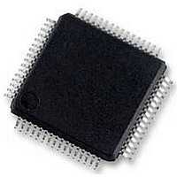
UPD78F0890GK(A)-GAJ-AX NEC, UPD78F0890GK(A)-GAJ-AX Datasheet - Page 367

UPD78F0890GK(A)-GAJ-AX
Manufacturer Part Number
UPD78F0890GK(A)-GAJ-AX
Description
8BIT MCU, 128K FLASH, 7K RAM, LQFP
Manufacturer
NEC
Datasheet
1.UPD78F0890GKA-GAJ-AX.pdf
(732 pages)
Specifications of UPD78F0890GK(A)-GAJ-AX
Controller Family/series
UPD78F
No. Of I/o's
55
Ram Memory Size
7KB
Cpu Speed
20MHz
No. Of Timers
10
No. Of Pwm
RoHS Compliant
Core Size
8bit
Program Memory Size
128KB
Oscillator Type
External, Internal
- Current page: 367 of 732
- Download datasheet (4Mb)
(a) Serial interface CSI10
Notes 1. Can be set as port function.
Remark
CSIE10 TRMD10 PM11
0
1
1
1
1
1
1
The relationship between the register settings and pins is shown below.
2. To use P10/SCK10/TxD61 as port pins, clear CKP10 to 0.
3. To use the slave mode, set CKS102, CKS101, and CKS100 to 1, 1, 1.
×:
CSIE10:
TRMD10:
CKP10:
CKS102, CKS101, CKS100:
PM1×:
P1×:
×
0
1
1
0
1
1
×
×
×
Note 1
Note 1
Note 1
1
1
1
1
Table 15-2. Relationship Between Register Settings and Pins (1/2)
×
×
×
P11
Note 1
Note 1
Note 1
×
×
×
×
CHAPTER 15 SERIAL INTERFACES CSI10 AND CSI11
PM12
×
×
×
Note 1
Note 1
Note 1
0
0
0
0
don’t care
Bit 7 of serial operation mode register 10 (CSIM10)
Bit 6 of CSIM10
Bit 4 of serial clock selection register 10 (CSIC10)
Bits 2 to 0 of CSIC10
Port mode register
Port output latch
×
×
×
P12
Note 1
Note 1
Note 1
0
0
0
0
User’s Manual U17554EJ4V0UD
PM10
×
Note 1
1
1
1
0
0
0
×
P10
Note 1
×
×
×
1
1
1
transmission
transmission/
transmission/
reception
reception
transmission
Operation
reception
reception
Master
Master
Master
CSI10
Slave
Slave
Slave
Stop
Note 3
Note 3
Note 3
SI10/RxD61/
RxD61/
RxD61/
RxD61/
SI10
SI10
SI10
SI10
P11
P11
P11
P11
Pin Function
SO10/P12 SCK10/TxD61/
SO10
SO10
SO10
SO10
P12
P12
P12
(input)
(input)
(input)
(output)
(output)
(output)
P10
TxD61/
SCK10
SCK10
SCK10
SCK10
SCK10
SCK10
P10
Note 2
Note 3
Note 3
Note 3
367
Related parts for UPD78F0890GK(A)-GAJ-AX
Image
Part Number
Description
Manufacturer
Datasheet
Request
R

Part Number:
Description:
16/8 bit single-chip microcomputer
Manufacturer:
NEC
Datasheet:

Part Number:
Description:
Dual audio power amp circuit
Manufacturer:
NEC
Datasheet:

Part Number:
Description:
Dual comparator
Manufacturer:
NEC
Datasheet:

Part Number:
Description:
MOS type composite field effect transistor
Manufacturer:
NEC
Datasheet:

Part Number:
Description:
50 V/100 mA FET array incorporating 2 N-ch MOSFETs
Manufacturer:
NEC
Datasheet:

Part Number:
Description:
6-pin small MM high-frequency double transistor
Manufacturer:
NEC
Datasheet:

Part Number:
Description:
6-pin small MM high-frequency double transistor
Manufacturer:
NEC
Datasheet:

Part Number:
Description:
6-pin small MM high-frequency double transistor
Manufacturer:
NEC
Datasheet:

Part Number:
Description:
6-pin small MM high-frequency double transistor
Manufacturer:
NEC
Datasheet:

Part Number:
Description:
Twin transistors equipped with different model chips(6P small MM)
Manufacturer:
NEC
Datasheet:

Part Number:
Description:
Bipolar analog integrated circuit
Manufacturer:
NEC
Datasheet:


