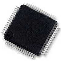
UPD78F0890GK(A)-GAJ-AX NEC, UPD78F0890GK(A)-GAJ-AX Datasheet - Page 122

UPD78F0890GK(A)-GAJ-AX
Manufacturer Part Number
UPD78F0890GK(A)-GAJ-AX
Description
8BIT MCU, 128K FLASH, 7K RAM, LQFP
Manufacturer
NEC
Datasheet
1.UPD78F0890GKA-GAJ-AX.pdf
(732 pages)
Specifications of UPD78F0890GK(A)-GAJ-AX
Controller Family/series
UPD78F
No. Of I/o's
55
Ram Memory Size
7KB
Cpu Speed
20MHz
No. Of Timers
10
No. Of Pwm
RoHS Compliant
Core Size
8bit
Program Memory Size
128KB
Oscillator Type
External, Internal
- Current page: 122 of 732
- Download datasheet (4Mb)
(4) A/D port configuration register (ADPC)
122
This register switches the P80/ANI0 to P87/ANI7 and P90/ANI8 to P93/ANI11 pins to digital I/O of port or analog
input of A/D converter.
ADPC can be set by a 1-bit or 8-bit memory manipulation instruction.
Reset signal generation clears this register to 00H.
Cautions 1. Set the channel used for A/D conversion to the input mode by using port mode register
ADPC3 ADPC2 ADPC1 ADPC0
0
0
0
0
0
0
0
0
1
1
1
1
1
Other than above
2. If data is written to ADPC, a wait cycle is generated. Do not write data to ADPC when the
0
0
0
0
1
1
1
1
0
0
0
0
1
8 (PM8) and port mode register 9 (PM9).
CPU is operating on the subsystem clock and the peripheral hardware clock is stopped.
For details, see CHAPTER 31 CAUTIONS FOR WAIT.
0
0
1
1
0
0
1
1
0
0
1
1
0
Table 5-6. Format of A/D Port Configuration Register (ADPC)
0
1
0
1
0
1
0
1
0
1
0
1
0
ANI11
Setting prohibited
P93/
D
A
A
A
A
A
A
A
A
A
A
A
A
ANI10
P92/
CHAPTER 5 PORT FUNCTIONS
A
A
A
A
A
A
A
A
A
A
A
D
D
User’s Manual U17554EJ4V0UD
ANI9
P91/
A
A
A
A
A
A
A
A
A
A
D
D
D
Analog input (A)/ digital input (D) switching
ANI8
P90/
A
A
A
A
A
A
A
A
A
D
D
D
D
ANI7
P87/
A
A
A
A
A
A
A
A
D
D
D
D
D
ANI6
P86/
D
D
D
D
D
D
A
A
A
A
A
A
A
ANI5
P85/
D
D
D
D
D
D
D
A
A
A
A
A
A
ANI4
P84/
D
D
D
D
D
D
D
D
A
A
A
A
A
ANI3
P83/
A
A
A
D
D
D
D
D
D
D
D
D
A
ANI2
P82/
A
A
A
D
D
D
D
D
D
D
D
D
D
ANI1
P81/
A
A
D
D
D
D
D
D
D
D
D
D
D
ANI0
P80/
D
D
D
D
D
A
D
D
D
D
D
D
D
Related parts for UPD78F0890GK(A)-GAJ-AX
Image
Part Number
Description
Manufacturer
Datasheet
Request
R

Part Number:
Description:
16/8 bit single-chip microcomputer
Manufacturer:
NEC
Datasheet:

Part Number:
Description:
Dual audio power amp circuit
Manufacturer:
NEC
Datasheet:

Part Number:
Description:
Dual comparator
Manufacturer:
NEC
Datasheet:

Part Number:
Description:
MOS type composite field effect transistor
Manufacturer:
NEC
Datasheet:

Part Number:
Description:
50 V/100 mA FET array incorporating 2 N-ch MOSFETs
Manufacturer:
NEC
Datasheet:

Part Number:
Description:
6-pin small MM high-frequency double transistor
Manufacturer:
NEC
Datasheet:

Part Number:
Description:
6-pin small MM high-frequency double transistor
Manufacturer:
NEC
Datasheet:

Part Number:
Description:
6-pin small MM high-frequency double transistor
Manufacturer:
NEC
Datasheet:

Part Number:
Description:
6-pin small MM high-frequency double transistor
Manufacturer:
NEC
Datasheet:

Part Number:
Description:
Twin transistors equipped with different model chips(6P small MM)
Manufacturer:
NEC
Datasheet:

Part Number:
Description:
Bipolar analog integrated circuit
Manufacturer:
NEC
Datasheet:


