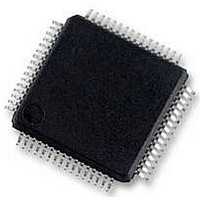
UPD78F0890GK(A)-GAJ-AX NEC, UPD78F0890GK(A)-GAJ-AX Datasheet - Page 729

UPD78F0890GK(A)-GAJ-AX
Manufacturer Part Number
UPD78F0890GK(A)-GAJ-AX
Description
8BIT MCU, 128K FLASH, 7K RAM, LQFP
Manufacturer
NEC
Datasheet
1.UPD78F0890GKA-GAJ-AX.pdf
(732 pages)
Specifications of UPD78F0890GK(A)-GAJ-AX
Controller Family/series
UPD78F
No. Of I/o's
55
Ram Memory Size
7KB
Cpu Speed
20MHz
No. Of Timers
10
No. Of Pwm
RoHS Compliant
Core Size
8bit
Program Memory Size
128KB
Oscillator Type
External, Internal
- Current page: 729 of 732
- Download datasheet (4Mb)
3rd
Edition
• Change of Figure and Note
Change of explanation in 24.5 (2) UART60
Table 24-4. Pin Connection
• Change of Table and Note 1
• Addition of REGC pin input voltage of Absolute Maximum Ratings
• Addition of I
• Addition of I
• Addition of RSTS = 1 and RSTS = 0 in the condition of 8 MHz internal oscillator
• Change of MAX. and MIN. value of 240 kHz internal oscillator
• Addition of Remark in (2) On-chip Internal Oscillator Characteristics
• Change of MAX. value of Output current, high in 4.0 V ≤ V
• Addition of Note 1 to 3 and change of Remark of Output current, high and Output current, low
• Change of MAX. value of Output current, high
• Addition of V
• Addition of I
• Change of MAX. value of Output voltage, low (I
• Change of Supply current, A/D converter operating current, Watchdog timer operating current, LVI
Figure 24-7. Communication with Dedicated Flash Memory Programmer (UART60)
Change of Figure 24-8. FLMD0 Pin Connection Example
Change of explanation in 24.6.5 REGC pin
Change of explanation and Caution 3 in 24.6.6 Other signal pins
Change of explanation in 24.6.7 Power supply
Change of Note 1 in Table 24-7. Communication Modes
Addition of 24.8 Security Settings
Addition of 24.9 Processing Time for Each Command When PG-FP4 Is Used (Reference)
Change of Figure 24-16. Self-Programming Procedure
Addition of Table 24-14. Processing Time and Interrupt Response Time for Self Programming Sample Library
Change of 24.11 Boot swap function
Change of Caution in 25.1 Outline of Functions
Addition of Note and Caution in Figure 25-2. Connection Circuit Example (When QB-78K0MINI Is Not Used) and
Figure 25-3. Connection Circuit Example (When Using QB-78K0MINI: X1 and X2 Are Used)
Addition of Note in Figure 25-4. Connection Circuit Example (When Using QB-78K0MINI: Ports 31 and 32 Are
Used)
Addition of Figure 25-5. Connection of FLMD0 Pin for Self Programming by Means of On-Chip Debugging
Addition of 25.4 On-Chip Debug Security
Change of 25.5 Restrictions and Cautions on On-Chip Debug Function
27.1 Absolute Maximum Ratings
27.2 Oscillator Characteristics
27.3 DC Characteristics
operating current
OH2
OL2
OL
IH
4 of Input voltage, high
= 5.0 mA, 2.0 mA in the condition of Output voltage, low
and I
and I
OL3
OH3
in Output current, low of Absolute Maximum Ratings
in Output current, high of Absolute Maximum Ratings
APPENDIX D REVISION HISTORY
User’s Manual U17554EJ4V0UD
OL
= 1.0 mA and V
Description
DD
= EV
OL3
DD
, I
≤ 5.5 V and 2.7 V ≤ V
OL
= 5.0 mA, 3.0 mA, 1.0 mA)
DD
= EV
DD
< 4.0 V
(8/9)
729
Related parts for UPD78F0890GK(A)-GAJ-AX
Image
Part Number
Description
Manufacturer
Datasheet
Request
R

Part Number:
Description:
16/8 bit single-chip microcomputer
Manufacturer:
NEC
Datasheet:

Part Number:
Description:
Dual audio power amp circuit
Manufacturer:
NEC
Datasheet:

Part Number:
Description:
Dual comparator
Manufacturer:
NEC
Datasheet:

Part Number:
Description:
MOS type composite field effect transistor
Manufacturer:
NEC
Datasheet:

Part Number:
Description:
50 V/100 mA FET array incorporating 2 N-ch MOSFETs
Manufacturer:
NEC
Datasheet:

Part Number:
Description:
6-pin small MM high-frequency double transistor
Manufacturer:
NEC
Datasheet:

Part Number:
Description:
6-pin small MM high-frequency double transistor
Manufacturer:
NEC
Datasheet:

Part Number:
Description:
6-pin small MM high-frequency double transistor
Manufacturer:
NEC
Datasheet:

Part Number:
Description:
6-pin small MM high-frequency double transistor
Manufacturer:
NEC
Datasheet:

Part Number:
Description:
Twin transistors equipped with different model chips(6P small MM)
Manufacturer:
NEC
Datasheet:

Part Number:
Description:
Bipolar analog integrated circuit
Manufacturer:
NEC
Datasheet:


