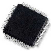
UPD78F0890GK(A)-GAJ-AX NEC, UPD78F0890GK(A)-GAJ-AX Datasheet - Page 634

UPD78F0890GK(A)-GAJ-AX
Manufacturer Part Number
UPD78F0890GK(A)-GAJ-AX
Description
8BIT MCU, 128K FLASH, 7K RAM, LQFP
Manufacturer
NEC
Datasheet
1.UPD78F0890GKA-GAJ-AX.pdf
(732 pages)
Specifications of UPD78F0890GK(A)-GAJ-AX
Controller Family/series
UPD78F
No. Of I/o's
55
Ram Memory Size
7KB
Cpu Speed
20MHz
No. Of Timers
10
No. Of Pwm
RoHS Compliant
Core Size
8bit
Program Memory Size
128KB
Oscillator Type
External, Internal
- Current page: 634 of 732
- Download datasheet (4Mb)
25.4 On-Chip Debug Security ID
OPTION BYTE) and an on-chip debug security ID setting area at 0085H to 008EH.
advance, because 0084H, 0085H to 008EH and 1084H, and 1085H to 108EH are switched.
25.5 Restrictions and Cautions on On-Chip Debug Function
will be unavailable for use.
pull-down resistor to the FLMD0 pin, and manipulate this pin based on high/high impedance levels, rather than on
high/low levels, when using ports for manipulation.
634
The 78K0/FE2 has an on-chip debug operation control flag in the flash memory at 0084H (see CHAPTER 23
When the boot swap function is used, also set a value that is the same as that of 1084H and 1085H to 108EH in
For details on the on-chip debug security ID, refer to the QB-78K0MINI User’s Manual (U17029E).
When setting to on-chip debugging mode via the normal port, without using pins X1 and X2, two of the user ports
A high-level signal is always output from to the FLMD0 pin during emulation when self-writing. Be sure to connect a
In order to realize on-chip debug function, use the following user resource.
For details, refer to the QB-78K0MINI User's Manual (U17029E).
(a) Flash memory area
(b) Internal extended RAM area
(c) Internal high-speed RAM area
Addresses 0x02 and 0x03
Addresses 0x7E and 0x7F (when using a software break)
Address 0x84
Addresses 0x85 to 0x8E
Addresses 0x8F to 0x18F: Standard value of program
(+256 bytes when using pseudo real-time RAM monitor function)
(when using a device with 10 or more SFRs the can be accessed in 16-bit units: +n (the number of
exceeding registers x 6 bytes))
Addresses 0xF7F0 to 0xF7FF
(when using pseudo real-time RAM monitor function)
7 bytes as stack area: Standard value of stack
(+2 bytes when using software breaks)
(+7 bytes when using pseudo real-time RAM monitor function)
0085H to 008EH
1085H to 108EH
Address
CHAPTER 25 ON-CHIP DEBUG FUNCTION
Table 25-1. On-Chip Debug Security ID
Any ID code of 10 bytes
User’s Manual U17554EJ4V0UD
On-Chip Debug Security ID
Related parts for UPD78F0890GK(A)-GAJ-AX
Image
Part Number
Description
Manufacturer
Datasheet
Request
R

Part Number:
Description:
16/8 bit single-chip microcomputer
Manufacturer:
NEC
Datasheet:

Part Number:
Description:
Dual audio power amp circuit
Manufacturer:
NEC
Datasheet:

Part Number:
Description:
Dual comparator
Manufacturer:
NEC
Datasheet:

Part Number:
Description:
MOS type composite field effect transistor
Manufacturer:
NEC
Datasheet:

Part Number:
Description:
50 V/100 mA FET array incorporating 2 N-ch MOSFETs
Manufacturer:
NEC
Datasheet:

Part Number:
Description:
6-pin small MM high-frequency double transistor
Manufacturer:
NEC
Datasheet:

Part Number:
Description:
6-pin small MM high-frequency double transistor
Manufacturer:
NEC
Datasheet:

Part Number:
Description:
6-pin small MM high-frequency double transistor
Manufacturer:
NEC
Datasheet:

Part Number:
Description:
6-pin small MM high-frequency double transistor
Manufacturer:
NEC
Datasheet:

Part Number:
Description:
Twin transistors equipped with different model chips(6P small MM)
Manufacturer:
NEC
Datasheet:

Part Number:
Description:
Bipolar analog integrated circuit
Manufacturer:
NEC
Datasheet:


