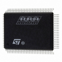
ST92F150CV1QB STMicroelectronics, ST92F150CV1QB Datasheet - Page 63

ST92F150CV1QB
Manufacturer Part Number
ST92F150CV1QB
Description
MCU 8BIT 128K FLASH 100PQFP
Manufacturer
STMicroelectronics
Series
ST9r
Datasheet
1.ST92F150CV1TB.pdf
(429 pages)
Specifications of ST92F150CV1QB
Core Processor
ST9
Core Size
8/16-Bit
Speed
24MHz
Connectivity
CAN, I²C, LIN, SCI, SPI
Peripherals
DMA, LVD, POR, PWM, WDT
Number Of I /o
77
Program Memory Size
128KB (128K x 8)
Program Memory Type
FLASH
Eeprom Size
1K x 8
Ram Size
4K x 8
Voltage - Supply (vcc/vdd)
4.5 V ~ 5.5 V
Data Converters
A/D 16x10b
Oscillator Type
Internal
Operating Temperature
-40°C ~ 105°C
Package / Case
100-QFP
Processor Series
ST92F15x
Core
ST9
Data Bus Width
8 bit, 16 bit
Data Ram Size
6 KB
Interface Type
CAN, I2C, SCI, SPI
Maximum Clock Frequency
24 MHz
Number Of Programmable I/os
80
Number Of Timers
5 x 16 bit
Operating Supply Voltage
4.5 V to 5.5 V
Maximum Operating Temperature
+ 105 C
Mounting Style
SMD/SMT
Development Tools By Supplier
ST92F150-EPB
Minimum Operating Temperature
- 40 C
On-chip Adc
16 bit x 10 bit
Lead Free Status / RoHS Status
Lead free / RoHS Compliant
Other names
497-4882
Available stocks
Company
Part Number
Manufacturer
Quantity
Price
Company:
Part Number:
ST92F150CV1QB
Manufacturer:
STMicroelectronics
Quantity:
10 000
- Current page: 63 of 429
- Download datasheet (8Mb)
PROTECTION STRATEGY (Cont’d)
NON VOLATILE PASSWORD (NVPWD1-0)
Address: 231FFF-231FFEh - Write Only
Delivery value: 1111 1111 (FFh)
Bit 7:0 = PWD[7:0]: Password bits 7:0 (Write On-
ly).
These bits must be programmed with the Non Vol-
atile Password that must be provided with the Set
Protection operation to disable (first write access)
or to reenable (second write access) the test and
EPB modes. The first write access fixes the pass-
word value and resets the TMDIS bit of NVWPR
(231FFDh). The second write access, with Pro-
gram Data matching with NVPWD[1:0] content, re-
sets the PWOK bit of NVWPR.
These two registers can be accessed only in write
mode (a read access returns FFh).
3.5.2 Temporary Unprotection
On user request the memory can be configured so
as to allow the temporary unprotection also of all
access protections bits of NVAPR (write protection
bits of NVWPR are always temporarily unprotecta-
ble).
PWD7 PWD6 PWD5 PWD4 PWD3 PWD2 PWD1 PWD0
7
ST92F124/F150/F250 - SINGLE VOLTAGE FLASH & E3 TM (EMULATED EEPROM)
6
5
4
3
2
1
0
Bit APEX can be temporarily disabled by execut-
ing the Set Protection operation and writing 1 into
this bit, but only if this write instruction is executed
from an internal memory (Flash and Test Flash ex-
cluded).
Bit APEE can be temporarily disabled by execut-
ing the Set Protection operation and writing 1 into
this bit, but only if this write instruction is executed
from the memory itself to unprotect (
Bits APRO and APBR can be temporarily disabled
through a direct write at NVAPR location, by over-
writing at 1 these bits, but only if this write instruc-
tion is executed from the memory itself to unpro-
tect.
To restore the access protections, reset the micro
or execute another Set Protection operation by
writing 0 to the desired bits.
Note: To restore all the protections previously en-
abled in the NVAPR or NVWPR register, read the
corresponding register.
When an internal memory (Flash, TestFlash or
E
through a DMA of a peripheral is forbidden (it re-
turns FFh). To read data in DMA mode from a pro-
tected memory, first it is necessary to temporarily
unprotect that memory.
The temporary unprotection allows also to update
a protected code.
Refer to the following figures to manage the Test/
EPB, Access and Write protection modes.
3 TM
) is protected in access, also the data access
E
3 TM
).
63/429
9
Related parts for ST92F150CV1QB
Image
Part Number
Description
Manufacturer
Datasheet
Request
R

Part Number:
Description:
BOARD PROGRAM FOR ST92F150 MCU
Manufacturer:
STMicroelectronics
Datasheet:

Part Number:
Description:
BOARD EVALUATION FOR ST9 SERIES
Manufacturer:
STMicroelectronics
Datasheet:

Part Number:
Description:
BOARD EMULATOR FOR ST9 SERIES
Manufacturer:
STMicroelectronics
Datasheet:

Part Number:
Description:
MCU, MPU & DSP Development Tools ST9 Dedication Board
Manufacturer:
STMicroelectronics
Datasheet:

Part Number:
Description:
STMicroelectronics [RIPPLE-CARRY BINARY COUNTER/DIVIDERS]
Manufacturer:
STMicroelectronics
Datasheet:

Part Number:
Description:
STMicroelectronics [LIQUID-CRYSTAL DISPLAY DRIVERS]
Manufacturer:
STMicroelectronics
Datasheet:

Part Number:
Description:
BOARD EVAL FOR MEMS SENSORS
Manufacturer:
STMicroelectronics
Datasheet:

Part Number:
Description:
NPN TRANSISTOR POWER MODULE
Manufacturer:
STMicroelectronics
Datasheet:

Part Number:
Description:
TURBOSWITCH ULTRA-FAST HIGH VOLTAGE DIODE
Manufacturer:
STMicroelectronics
Datasheet:

Part Number:
Description:
Manufacturer:
STMicroelectronics
Datasheet:

Part Number:
Description:
DIODE / SCR MODULE
Manufacturer:
STMicroelectronics
Datasheet:

Part Number:
Description:
DIODE / SCR MODULE
Manufacturer:
STMicroelectronics
Datasheet:


