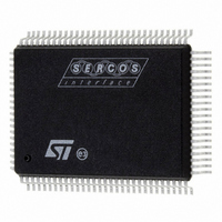
ST92F150CV1QB STMicroelectronics, ST92F150CV1QB Datasheet - Page 136

ST92F150CV1QB
Manufacturer Part Number
ST92F150CV1QB
Description
MCU 8BIT 128K FLASH 100PQFP
Manufacturer
STMicroelectronics
Series
ST9r
Datasheet
1.ST92F150CV1TB.pdf
(429 pages)
Specifications of ST92F150CV1QB
Core Processor
ST9
Core Size
8/16-Bit
Speed
24MHz
Connectivity
CAN, I²C, LIN, SCI, SPI
Peripherals
DMA, LVD, POR, PWM, WDT
Number Of I /o
77
Program Memory Size
128KB (128K x 8)
Program Memory Type
FLASH
Eeprom Size
1K x 8
Ram Size
4K x 8
Voltage - Supply (vcc/vdd)
4.5 V ~ 5.5 V
Data Converters
A/D 16x10b
Oscillator Type
Internal
Operating Temperature
-40°C ~ 105°C
Package / Case
100-QFP
Processor Series
ST92F15x
Core
ST9
Data Bus Width
8 bit, 16 bit
Data Ram Size
6 KB
Interface Type
CAN, I2C, SCI, SPI
Maximum Clock Frequency
24 MHz
Number Of Programmable I/os
80
Number Of Timers
5 x 16 bit
Operating Supply Voltage
4.5 V to 5.5 V
Maximum Operating Temperature
+ 105 C
Mounting Style
SMD/SMT
Development Tools By Supplier
ST92F150-EPB
Minimum Operating Temperature
- 40 C
On-chip Adc
16 bit x 10 bit
Lead Free Status / RoHS Status
Lead free / RoHS Compliant
Other names
497-4882
Available stocks
Company
Part Number
Manufacturer
Quantity
Price
Company:
Part Number:
ST92F150CV1QB
Manufacturer:
STMicroelectronics
Quantity:
10 000
- Current page: 136 of 429
- Download datasheet (8Mb)
ST92F124/F150/F250 - RESET AND CLOCK CONTROL UNIT (RCCU)
CLOCK CONTROL REGISTERS (Cont’d)
PLL CONFIGURATION REGISTER (PLLCONF)
R246 - Read/Write
Register Page: 55
Reset Value: 0x00 x111
Bit 7 = FREEN: PLL Free Running Mode Enable
0: PLL Free Running Mode disabled
1: PLL Free Running Mode enabled
When this bit is set, even if the DX[2:0] bits are all
set to 1, the PLL is not stopped but provides a slow
frequency back-up clock, selectable by the
CSU_CKSEL bit of the CLK_FLAG register (with-
out needing to have the LOCK bit equal to ‘1’).
Bits 5:4 = MX[1:0]: PLL Multiplication Factor.
Refer to
WARNING: After these bits are modified, take
care that the PLL lock-in time has elapsed before
setting the CSU_CKSEL bit in the CLK_FLAG reg-
ister.
Bits 2:0 = DX[2:0]: PLL output clock divider factor.
Refer to
136/429
9
FREEN
7
Table 29
Table 30
0
MX1
for multiplier settings.
for divider settings.
MX0
0
DX2
DX1
DX0
0
Table 29. PLL Multiplication Factors
Table 30. PLL Divider Factors
DX2
0
0
0
0
1
1
1
1
MX1
1
0
1
0
DX1
0
0
1
1
0
0
1
1
MX0
0
0
1
1
DX0
0
1
0
1
0
1
0
1
(PLL OFF, Reset State)
PLL CLOCK/1
PLL CLOCK/2
PLL CLOCK/3
PLL CLOCK/4
PLL CLOCK/5
PLL CLOCK/6
PLL CLOCK/7
CLOCK2 x
CLOCK2
CK
14
10
8
6
Related parts for ST92F150CV1QB
Image
Part Number
Description
Manufacturer
Datasheet
Request
R

Part Number:
Description:
BOARD PROGRAM FOR ST92F150 MCU
Manufacturer:
STMicroelectronics
Datasheet:

Part Number:
Description:
BOARD EVALUATION FOR ST9 SERIES
Manufacturer:
STMicroelectronics
Datasheet:

Part Number:
Description:
BOARD EMULATOR FOR ST9 SERIES
Manufacturer:
STMicroelectronics
Datasheet:

Part Number:
Description:
MCU, MPU & DSP Development Tools ST9 Dedication Board
Manufacturer:
STMicroelectronics
Datasheet:

Part Number:
Description:
STMicroelectronics [RIPPLE-CARRY BINARY COUNTER/DIVIDERS]
Manufacturer:
STMicroelectronics
Datasheet:

Part Number:
Description:
STMicroelectronics [LIQUID-CRYSTAL DISPLAY DRIVERS]
Manufacturer:
STMicroelectronics
Datasheet:

Part Number:
Description:
BOARD EVAL FOR MEMS SENSORS
Manufacturer:
STMicroelectronics
Datasheet:

Part Number:
Description:
NPN TRANSISTOR POWER MODULE
Manufacturer:
STMicroelectronics
Datasheet:

Part Number:
Description:
TURBOSWITCH ULTRA-FAST HIGH VOLTAGE DIODE
Manufacturer:
STMicroelectronics
Datasheet:

Part Number:
Description:
Manufacturer:
STMicroelectronics
Datasheet:

Part Number:
Description:
DIODE / SCR MODULE
Manufacturer:
STMicroelectronics
Datasheet:

Part Number:
Description:
DIODE / SCR MODULE
Manufacturer:
STMicroelectronics
Datasheet:


