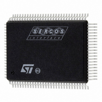
ST92F150CV1QB STMicroelectronics, ST92F150CV1QB Datasheet - Page 385

ST92F150CV1QB
Manufacturer Part Number
ST92F150CV1QB
Description
MCU 8BIT 128K FLASH 100PQFP
Manufacturer
STMicroelectronics
Series
ST9r
Datasheet
1.ST92F150CV1TB.pdf
(429 pages)
Specifications of ST92F150CV1QB
Core Processor
ST9
Core Size
8/16-Bit
Speed
24MHz
Connectivity
CAN, I²C, LIN, SCI, SPI
Peripherals
DMA, LVD, POR, PWM, WDT
Number Of I /o
77
Program Memory Size
128KB (128K x 8)
Program Memory Type
FLASH
Eeprom Size
1K x 8
Ram Size
4K x 8
Voltage - Supply (vcc/vdd)
4.5 V ~ 5.5 V
Data Converters
A/D 16x10b
Oscillator Type
Internal
Operating Temperature
-40°C ~ 105°C
Package / Case
100-QFP
Processor Series
ST92F15x
Core
ST9
Data Bus Width
8 bit, 16 bit
Data Ram Size
6 KB
Interface Type
CAN, I2C, SCI, SPI
Maximum Clock Frequency
24 MHz
Number Of Programmable I/os
80
Number Of Timers
5 x 16 bit
Operating Supply Voltage
4.5 V to 5.5 V
Maximum Operating Temperature
+ 105 C
Mounting Style
SMD/SMT
Development Tools By Supplier
ST92F150-EPB
Minimum Operating Temperature
- 40 C
On-chip Adc
16 bit x 10 bit
Lead Free Status / RoHS Status
Lead free / RoHS Compliant
Other names
497-4882
Available stocks
Company
Part Number
Manufacturer
Quantity
Price
Company:
Part Number:
ST92F150CV1QB
Manufacturer:
STMicroelectronics
Quantity:
10 000
- Current page: 385 of 429
- Download datasheet (8Mb)
RCCU CHARACTERISTICS
(V
Note:
(1) Unless otherwise stated, typical data are based on T
production.
(2) Value guaranteed by design.
RCCU TIMING TABLE
(V
Note:
(1) Unless otherwise stated, typical data are based on T
production.
(2) To be valid, a RESET pulse must exceed t
(3) Depending on the delay between rising edge of RESET pin and the first rising edge of CLOCK1, the value can differ from the typical value
for +/- 1 CLOCK1 cycle.
Legend: T
BOOTROM TIMING TABLE
Note:
(1) Unless otherwise stated, typical data are based on T
production
(2) Refer to AN1528 for more details on BOOTROM code.
Symbol
Symbol
t
V
RSPH
DD
V
DD
V
I
Symbol
V
t
LKRS
t
t
HYRS
FRS
NFR
STR
IHRS
ILRS
IRS
t
BRE
= 5V ± 10%, T
= 5V ± 10%, T
(3)
osc
= Crystal Oscilllator Clock (CLOCK1) period.
RESET Input Filtered Pulse
RESET Input Non Filtered
Pulse
RESET Phase duration
STOP Restart duration
RESET Input High Level
RESET Input Low Level
Input Voltage Range
RESET Input Hysteresis
RESET Pin Input Leakage
BOOTROM Execution Duration
(see
(2)
Figure 65 on page
Parameter
Parameter
A
A
=
=
–
–
40°C to +125°C, C
40°C to +125°C, f
Parameter
NFR
137)
(2)
ST92F124/F150/F250 - ELECTRICAL CHARACTERISTICS
. All reset glitches with a duration shorter than t
DIV2 = 0
DIV2 = 1
(2)
Input Threshold
Input Threshold
0V < V
INTCLK
A
A
A
Comment
Comment
Load
= 25°C and V
= 25°C and V
= 25°C and V
IN
< V
= 50pF, f
= 24 MHz, unless otherwise specified)
DD
DD
DD
DD
f
= 5V. They are only reported for design guide lines not tested in
= 5V. They are only reported for design guide lines not tested in
Conditions
= 5V. They are only reported for design guide lines not tested in
OSC
INTCLK
0.75 x V
= 4MHz
Min
– 0.3
20
Min
– 1
= 24MHz, unless otherwise specified)
DD
FRS
Typ
20400
10200
20400
Typ
Value
Value
1
will be filtered
(2)
Typ Value
(1)
(1)
33
0.25 x V
V
DD
(1)
Max
Max
50
1
+ 0.3
DD
Unit
ms
385/429
Unit
T
T
Unit
ns
μs
μA
osc
osc
V
V
V
V
1
Related parts for ST92F150CV1QB
Image
Part Number
Description
Manufacturer
Datasheet
Request
R

Part Number:
Description:
BOARD PROGRAM FOR ST92F150 MCU
Manufacturer:
STMicroelectronics
Datasheet:

Part Number:
Description:
BOARD EVALUATION FOR ST9 SERIES
Manufacturer:
STMicroelectronics
Datasheet:

Part Number:
Description:
BOARD EMULATOR FOR ST9 SERIES
Manufacturer:
STMicroelectronics
Datasheet:

Part Number:
Description:
MCU, MPU & DSP Development Tools ST9 Dedication Board
Manufacturer:
STMicroelectronics
Datasheet:

Part Number:
Description:
STMicroelectronics [RIPPLE-CARRY BINARY COUNTER/DIVIDERS]
Manufacturer:
STMicroelectronics
Datasheet:

Part Number:
Description:
STMicroelectronics [LIQUID-CRYSTAL DISPLAY DRIVERS]
Manufacturer:
STMicroelectronics
Datasheet:

Part Number:
Description:
BOARD EVAL FOR MEMS SENSORS
Manufacturer:
STMicroelectronics
Datasheet:

Part Number:
Description:
NPN TRANSISTOR POWER MODULE
Manufacturer:
STMicroelectronics
Datasheet:

Part Number:
Description:
TURBOSWITCH ULTRA-FAST HIGH VOLTAGE DIODE
Manufacturer:
STMicroelectronics
Datasheet:

Part Number:
Description:
Manufacturer:
STMicroelectronics
Datasheet:

Part Number:
Description:
DIODE / SCR MODULE
Manufacturer:
STMicroelectronics
Datasheet:

Part Number:
Description:
DIODE / SCR MODULE
Manufacturer:
STMicroelectronics
Datasheet:


